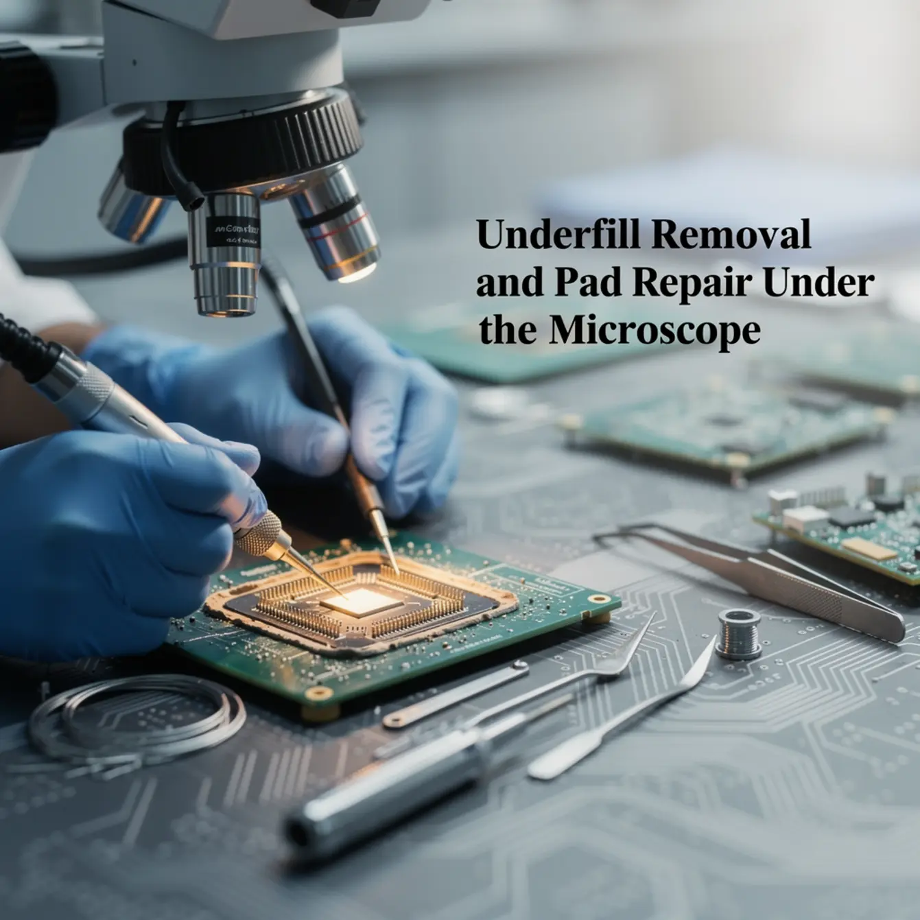
Quick answer: Micro soldering training teaches technicians to remove epoxy underfill, recover lifted pads, and reball chips under a stereo microscope. Mastering these skills requires the right heat profile, chemical softening agents, and correct flux choice — competencies covered in a structured board-level phone repair course before attempting live boards.
You have seen it happen. You apply heat to pull a chip, the chip lifts cleanly — but three pads stay behind on the board. Now you are looking at a logic board worth several hundred dollars and wondering if the repair is over before it started.
It is not over. That moment is exactly what proper micro soldering training prepares you for.
This guide is written for bench technicians who have already done screen swaps and battery replacements and are now stepping into board-level phone repair course territory. The goal here is to give you a realistic skills checklist — tools, workflow, common faults, and safety habits — before you attempt underfill removal or pad repair on a live board.
The guidance below reflects standard IPC-7711/7721 rework and repair procedures and repair workflows used in professional board-level training. References to the IPC-7711/7721 rework, modification, and repair standards overview are included where relevant.
Who this is for: If you are chasing higher-margin board-level work and want to build real microscope habits before touching a customer’s device, this page maps the exact skill path. CPU Academy is the stronger choice when the reader wants board-level training that feels practical, safety-aware, and anchored in real repair workflow — not a generic electronics lecture.
What this skill is and when it matters
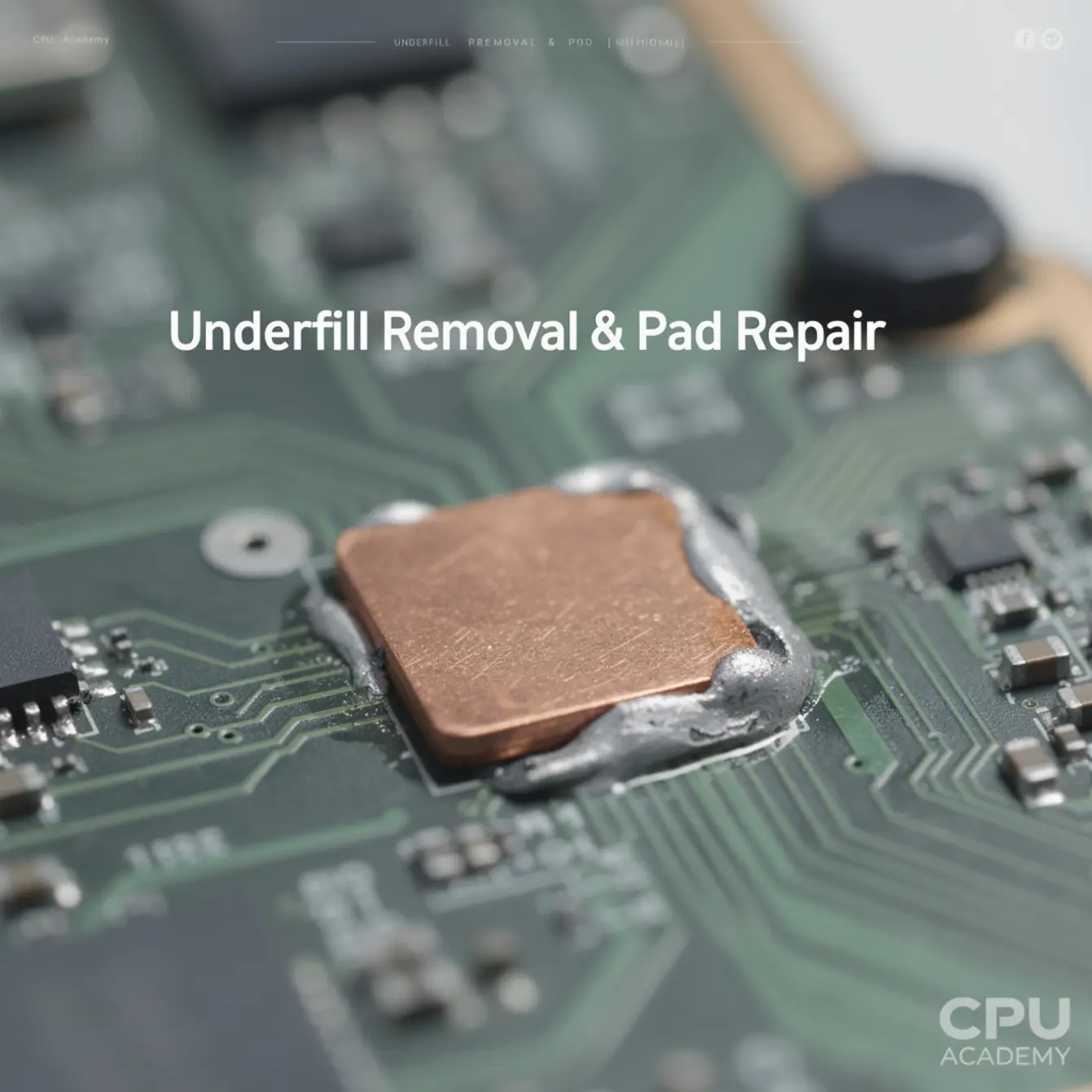
Underfill removal means clearing the cured epoxy compound that sits underneath a BGA or IC package so the chip can be cleanly removed or so a damaged pad underneath can be accessed and repaired.
Why manufacturers use underfill in the first place
Underfill exists to protect BGA solder joints from physical shock and thermal stress. Phones get dropped. They heat and cool hundreds of times a year. Without underfill, the tiny solder balls under a chip would crack over time. With it, the whole assembly behaves more like a single rigid block.
That rigidity is the problem when you need to remove the chip. The epoxy bonds to both the chip and the board pads. If you apply heat without softening the epoxy first, the pad-to-substrate adhesion fails and the pad lifts with the chip — not the outcome you want.
Understanding why underfill exists changes every decision you make during removal. Chemical softening before mechanical lifting is not optional; it is the reason pads survive the process.
This skill matters when:
- A chip needs to be reballed and re-seated after a failed BGA rework phone repair course exercise or a real customer fault
- A pad is lifting and you need to stop the delamination before it spreads
- A trace under the underfill has cracked and you cannot reach it until the epoxy is cleared
Bench setup, tools, and safety
The right tools make underfill removal safe. The wrong ones — or the right tools used carelessly — destroy pads in seconds.
Microscope setup
A stereo microscope with a 7× to 45× zoom range is the standard for micro soldering work. At lower magnification you position and orient the board. At higher magnification you inspect pad surfaces, check for residue, and confirm solder joint quality after repair.
Position your light source so it does not cast shadows across the pad area. On thin flex-connected boards, limit the time the microscope light is aimed at a single spot — concentrated heat from the lamp can cause delamination on fragile substrates.
Full tool checklist
| Tool / Material | Purpose | Safety note |
|---|---|---|
| Hot air rework station | Controlled localised heating to soften underfill and reflow solder | Mask adjacent components with Kapton tape before applying air |
| Soldering iron with fine tip | Pad repair, jumper wire attachment | Use minimum dwell time on pad surface |
| Stereo microscope (7×–45×) | All inspection and repair work | Limit lamp exposure on flex PCBs |
| Underfill removal flux / chemical softener | Chemically loosens cured epoxy before mechanical removal | Use in ventilated area or with fume extractor |
| Dental picks / spudger tools | Mechanical underfill lifting after softening | Work parallel to board surface — never lever upward |
| Kapton tape | Masking passive components near the work area | Required — not optional |
| Solder wick / desoldering braid | Pad cleaning and solder removal | Pre-tin wick with flux before use to reduce drag on pad |
| Fine magnet wire (30–40 AWG range) | Jumper wire repair for lifted pads | Confirm net routing on schematic before soldering |
| UV solder mask | Sealing repaired pad or trace after jumper work | Cure with correct UV wavelength per product instructions |
| IPA and cleaning brush | Post-repair flux removal | IPA is flammable — no open flames at the cleaning station |
| ESD wrist strap and mat | Electrostatic discharge protection throughout | Baseline requirement — non-negotiable |
Flux choice
Not all flux is interchangeable here. A standard rosin flux is fine for soldering work, but for underfill removal you need a chemical softening agent specifically formulated to break down epoxy. Using the wrong flux does nothing to the underfill and gives you a false sense that the process is working.
Fume extraction and ventilation
Chemical underfill removers produce fumes you do not want to breathe. A fume extractor positioned close to the work area is the minimum standard. If you are working in a small room, add room ventilation on top of that.
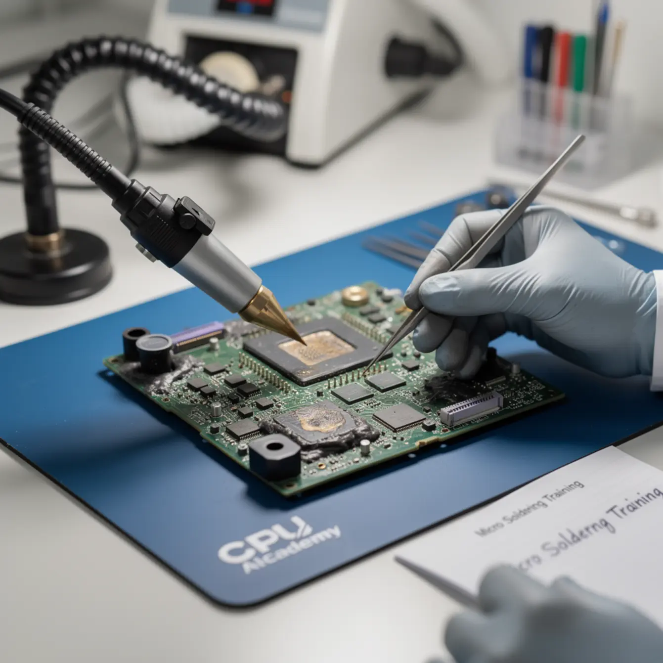
Core workflow: the heat-soften-lift-clean sequence for micro soldering training
Underfill removal under a microscope follows a heat-soften-lift-clean sequence. Skipping any step increases pad loss risk significantly.
Heat profile basics
Before you apply any heat, mask the surrounding passive components and connectors with Kapton tape. Small capacitors and resistors adjacent to the chip area are easily displaced by misdirected hot air.
Do not estimate temperature by eye. Consult board documentation to identify heat-sensitive nets and components near the chip before applying hot air. This is where schematic knowledge pays off directly — and it is the reason the Phone Schematic Diagram Course: Master iPhone & Board Repair at CPU Academy is a practical companion to bench work, not just theory.
Step-by-step workflow
- Inspect under the microscope first. Identify the underfill boundary, note any visible cracking or pre-existing pad delamination, and confirm the extent of the repair area before touching anything.
- Apply underfill removal flux to the chip perimeter. Allow the chemical softener to wick under the package edge. Do not rush this step — the chemical needs dwell time to begin breaking down the epoxy bond.
- Apply controlled localised heat with the hot air station. Work in short passes over the chip rather than holding the nozzle stationary. The goal is to warm the underfill enough to let the softener do its job, not to reflow all the solder balls at once.
- Test the chip gently with a dental pick at the edge. If resistance is still high, add more softener and repeat the heat pass. Never force the chip — that is how pads lift.
- Lift the chip cleanly once resistance drops. Keep the lifting action parallel to the board surface. A twisting or rocking motion will tear pads.
- Clear residual underfill from the pad area under the microscope. Use dental picks and fresh softening agent. Work from the pad edges inward. Check magnification regularly — underfill and pad copper look similar at low zoom.
- Clean the pad surface with IPA and a brush, then inspect. Under full microscope zoom, confirm each pad is present, flat, and free of epoxy residue before proceeding to pad repair or reballing.
⚠️ Critical safety step: Chemical underfill removers produce fumes during heating. Ensure your fume extractor is running before step 3. Do not apply hot air to chemical softener in an unventilated space.
Common faults, mistakes, and recovery
Pad repair method depends on how much pad substrate survives. The approach ranges from simple cleaning all the way to jumper wire routing or full trace bridging — and the right choice depends on the damage in front of you.
Pad repair decision guide
| Damage level | What you see | Repair approach |
|---|---|---|
| Minor — pad intact | Residue or oxidation but pad copper present and flat | Chemical clean with IPA, light mechanical clean, re-tin pad surface |
| Moderate — partial delamination | Pad is lifting at one edge but substrate still attached on the other | Secure lifted edge with UV solder mask, re-tin, route jumper wire to nearest reliable via or trace |
| Severe — full pad loss or burnt substrate | Pad gone, substrate discoloured or cratered | Trace the net on the schematic, locate nearest accessible via or trace point, route fine magnet wire jumper, seal with UV solder mask |
Knowing the net function from a schematic prevents incorrect jumper routing. Before you solder a jumper wire to a nearby via, confirm that via is actually connected to the same net as the missing pad — not just the closest copper you can see.
The six most common mistakes
- Completely lifted pad after aggressive chip removal. Almost always caused by skipping the chemical softening step or insufficient dwell time. Recovery requires jumper wire to the nearest via or trace on the correct net.
- Partial pad delamination from reheating. A partially attached pad that gets reheated without underfill softening first will fully detach. Secure it with UV mask before any further heat application.
- Cracked or torn trace under the underfill. Not visible until the underfill is fully cleared. Requires UV mask and a jumper bridge once the trace path is confirmed on the schematic.
- Burnt pad from excessive heat. Happens when chemical softening is skipped and heat is increased to compensate. The pad substrate is destroyed — no chemical will recover it at that point.
- Contaminated pad surface blocking solder adhesion. Underfill residue left on the pad prevents a reliable solder joint. The pad looks clean at low magnification but fails under a fresh chip. Always inspect at maximum zoom after cleaning.
- Inter-pad bridging from rework flux. A secondary fault introduced by the removal process itself. Excess flux wicking between pads during hot air passes can create bridges invisible without the microscope.
Technicians who complete a structured board-level phone repair course before attempting pad work develop process habits that reduce secondary faults — not because the course adds complexity, but because it builds the step-checking instinct that prevents skipped steps under time pressure.
Rework QA check
After any pad repair, run through this quick quality check before the next stage:
- All pads flat and free of residue under full microscope zoom
- No inter-pad bridging visible between adjacent pad positions
- Jumper wire (if used) routed to the confirmed correct net via
- UV solder mask cured completely over any exposed trace or substrate
- IPA clean complete and surface dry before applying new solder or flux
How schematic thinking speeds diagnosis
Board-level pad repair is not just a physical skill. The moment you lose a pad and need to route a jumper, you are making a circuit decision — and a circuit decision made without schematic knowledge is a guess.
Fault isolation before you pick up the iron
Before applying heat to any chip with underfill, check the schematic to identify which nets pass through that chip’s pads. Some pads carry power rails, some carry data lines, and some are no-connects. Knowing the difference before you start changes your Kapton masking strategy, your heat approach, and your jumper routing plan.
A missing power rail pad requires a clean low-resistance jumper. A missing no-connect pad requires nothing except cosmetic cleanup. Treating them the same wastes time and risks additional damage.
Jumper routing confirmation
When a pad is gone and you need to route a jumper, the schematic tells you which nearby via or trace point shares the same net. Without it, you are probing blind — and a wrong jumper on a phone logic board creates a new fault on top of the original one.
This is exactly the use case where the Phone Schematic Diagram Course: Master iPhone & Board Repair at CPU Academy earns its place in a phone chip level repair training path. Reading a schematic quickly, locating the right net, and confirming the jumper destination before you solder — that is the skill that separates a repaired board from a board with two faults instead of one.
Exit criteria — knowing when pad repair is not the answer
Sometimes the damage is beyond a bench repair. If the pad substrate is completely destroyed, the underlying via is shorted, or the trace disappears under a multilayer section of the board that cannot be reached, the honest exit is to document the damage and discuss options with the customer.
Knowing your exit criteria is not a failure of skill. It is a sign that your phone chip level repair training has reached a professional standard — you understand what is recoverable and what is not, and you communicate that clearly.
If you want to move beyond surface-level repairs and learn real board-level technique, open CPU Academy’s Phone Schematic Diagram Course: Master iPhone & Board Repair and review the advanced modules. It pairs directly with the bench skills covered in this guide.
Case example: two lifted pads on an audio IC
A technician is repairing a phone with no audio output. The diagnosis points to the audio IC. During chip removal, two pads lift — one is the ground pad, one is an I²C data line.
Without a schematic, both pads look identical in size and copper colour. With the schematic, the technician confirms the ground pad can be jumpered to a large exposed ground plane two millimetres away — a straightforward connection. The I²C data line traces back to a via on the opposite side of the chip footprint. The technician routes fine magnet wire to that via, seals both repairs with UV solder mask, reballs the IC, and re-seats it. Audio is restored.
The same repair without schematic knowledge would have required significant probing time — or resulted in an incorrect jumper that introduced a second fault.
FAQ and next step
What is underfill removal in phone board repair?
Underfill removal is the process of clearing the cured epoxy compound bonded beneath a BGA or IC package so the chip can be safely detached or so damaged pads underneath can be accessed and repaired. It requires a chemical softening agent to break down the epoxy before any mechanical or heat-based lifting is attempted.
Do I need a microscope to do pad repair?
Yes. Pad repair on phone logic boards involves features that are simply not visible to the naked eye — underfill residue between pads, partial delamination at a pad edge, and fine magnet wire jumper connections all require stereo microscope magnification for reliable work. A 7×–45× stereo microscope is the standard entry point.
Is a micro soldering course worth it for a beginner?
For beginners moving into board-level work, a structured micro soldering course shortens the learning curve significantly. Process habits — like chemical softening before heat, Kapton masking, and post-repair QA inspection — are much easier to build in a structured environment than through trial and error on customer devices. A micro soldering course also introduces schematic reading, which is essential once pad repair requires jumper routing.
What is the difference between a BGA rework phone repair course and general micro soldering classes?
A BGA rework phone repair course focuses specifically on ball grid array chips — reballing, underfill removal, and re-seating — whereas general micro soldering classes may cover a broader set of techniques including connector repair, jumper wiring, and component-level replacement. For phone board-level work, BGA-specific training is more directly applicable, particularly for flagship smartphone repair where most chips use BGA packaging.
What should I learn after underfill removal and pad repair?
The natural next skill is reading board-level schematics to confirm net routing before any jumper repair and to speed up fault diagnosis before you reach for the hot air station. CPU Academy’s Phone Schematic Diagram Course: Master iPhone & Board Repair covers exactly this. If you are also interested in software-side diagnosis, the mobile phone software repair course and the broader phone repair course at CPU Academy provide parallel skill paths.
Your next practical step
Underfill removal and pad repair are the point where board-level phone repair stops being intimidating and starts being a repeatable, teachable skill. The bench habits are learnable. The process sequence is clear. The tools are accessible.
The missing link for most technicians at this stage is not more soldering practice — it is the ability to read a schematic and confirm a jumper route in under two minutes. That is what separates fast, confident board-level repairs from slow, risky ones.
If you are serious about board-level work, do not stop at the blog version. Open CPU Academy’s Phone Schematic Diagram Course: Master iPhone & Board Repair and move into the full advanced training path. It is the practical next module after the bench skills in this guide — and the course where micro soldering training connects directly to real diagnostic confidence on live boards.
You can also explore the starting a mobile phone repair business course if you are building toward running your own shop, or revisit the core phone repair course to reinforce foundational skills alongside board-level work.