Quick answer: Micro soldering training teaches technicians to work at the board level — removing, cleaning, and reflowing BGA chips using stencils and solder balls. For stencil and reball work specifically, beginners need to understand stencil aperture types, correct flux application, and heat profiles before they attempt any live repair.
Picture a dead iPhone that powers on but shows no display. Or a board where the NAND chip just won’t seat after harvesting. Both jobs look impossible until you understand what’s actually happening at the pad level. Once the workflow clicks — stencil, flux, balls, reflow, inspect — the mystery goes away fast.
This guide is written for technicians who already handle basic phone repair and are ready to step into board-level work. It covers the practical stuff: choosing the right stencil, setting up your bench safely, running a clean reball from start to finish, and catching your faults before they turn into wasted chips.
What this skill is and when it matters
BGA stands for Ball Grid Array. It describes any chip that connects to the board through a grid of tiny solder balls on its underside rather than visible pins around the edges. The NAND flash, PMIC, CPU/AP, and baseband processor in modern smartphones are all BGA devices.
Solder joints fail for two main reasons: physical stress from a drop, a flex, or water damage, and plain old age-related fatigue. When that happens, the chip loses contact with the board even though the chip itself may be perfectly fine. Reballing restores those contacts by pulling the old solder, cleaning the pads, and laying down fresh solder balls.
You also reball when you harvest a chip off a donor board. That chip comes to you with old, uneven solder on it. Before it goes onto a new board, every ball needs to be clean and consistent. That’s exactly what the stencil and reball process delivers.
This is one of the highest-value skills in phone repair. BGA rework jobs can’t be handed off to the parts counter. They need a trained technician, which is why putting time and money into a structured micro soldering course pays back quickly for anyone serious about chip-level work.
Bench setup, tools, and safety
The minimum tool set
You don’t need a factory SMT line to do this well. You do need the right tools used the right way. Here’s the realistic minimum for beginner reball work:
| Tool | Purpose | Beginner note |
|---|---|---|
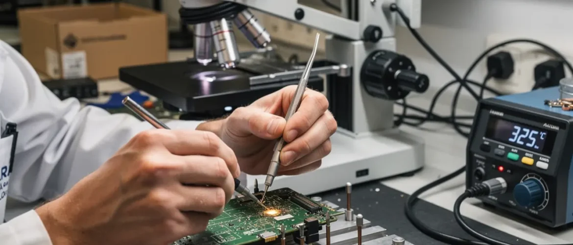
| Hot-air rework station | Remove and reflow chips | Temperature and airflow control are both critical |
| BGA reball stencil | Holds solder balls in the correct pattern | Chip-specific stencils give better results than universal ones |
| Solder balls (lead-free SAC) | Replacement BGA balls | Match ball diameter to the chip spec |
| No-clean flux paste | Bonds balls to pads during reflow | Thin, even layer — more is not better |
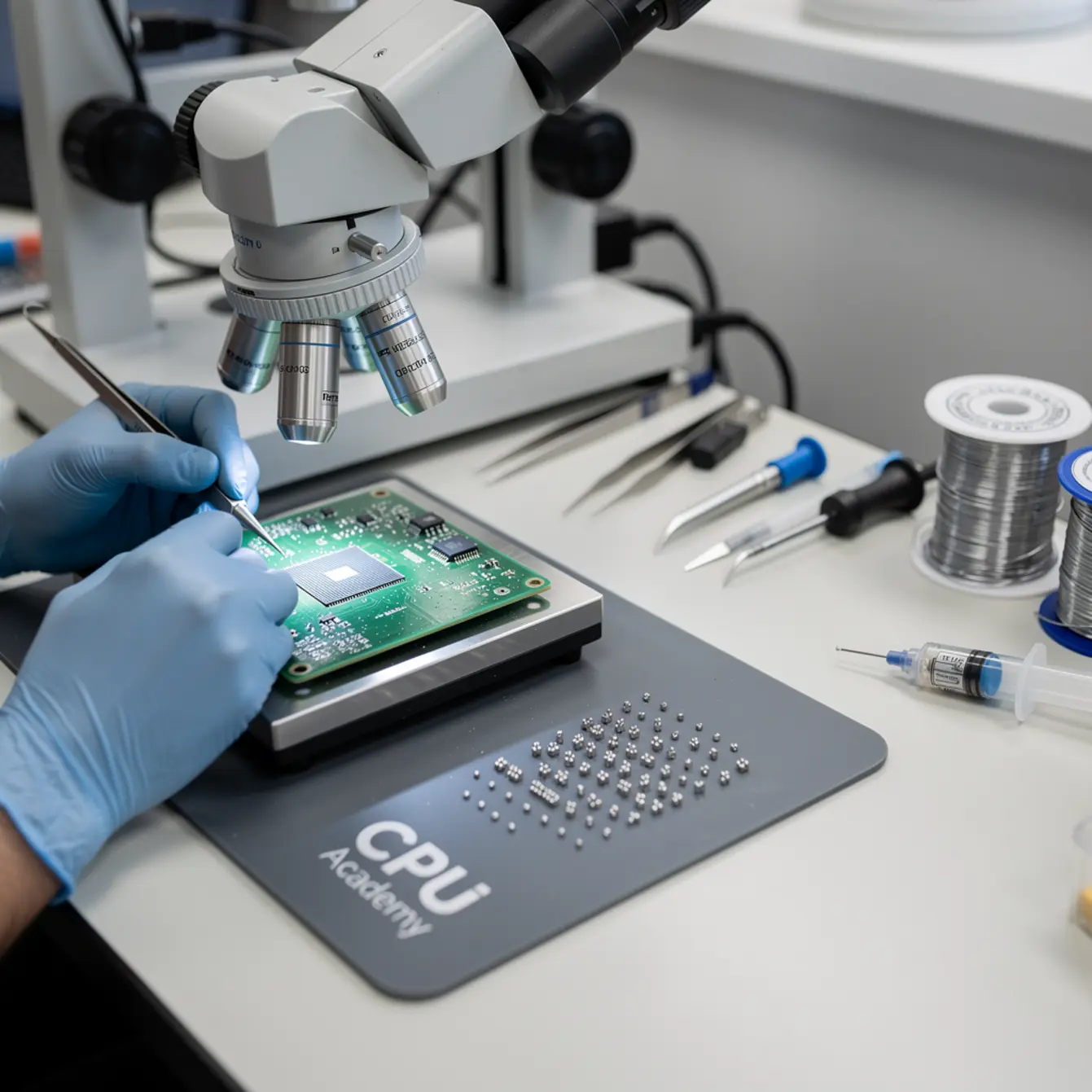
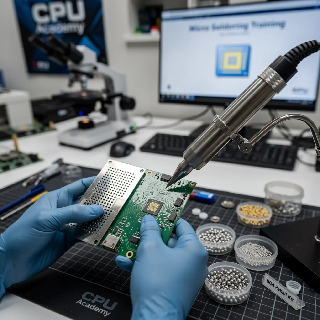
| Trinocular stereo microscope | Inspect pads and finished ball array | Non-negotiable for QA at ball level |
| Chip cleaning braid + IPA | Remove old solder and flux residue | Clean pads are the foundation of a good reball |
| PCB holder / reball jig | Secure the chip while stencil is placed | Prevents movement during ball placement |
| ESD mat and wrist strap | Prevent static discharge to live components | Use every time — ESD damage is silent |
Microscope setup
Set up your microscope so both hands stay free while you look through it. Most beginners get this wrong by positioning the scope too high, which forces awkward wrist angles right under a hot-air nozzle. Start at the lowest zoom setting until you’re comfortable, then step up as you inspect individual balls. Good microscope posture isn’t a small thing — hunching over a badly positioned scope for two hours will cost you accuracy before the session is over.
Safety basics at the bench
Hot-air rework runs at temperatures that burn skin instantly and can ignite flux fumes. Work in a ventilated space or pull fumes away from your face with a dedicated extractor. Keep Kapton tape ready to shield any components sitting close to your reball target — it handles heat well, peels off cleanly, and costs almost nothing per job.
Core workflow: the reball sequence — your micro soldering training in practice
The reball sequence is the same every time you do it. Skipping a step is where beginner mistakes come from. Here is the full procedure:
✅ BGA Reball Checklist
- Clean old solder from all chip pads using braid and IPA
- Inspect pads under the microscope — no lifted pads, no residue
- Apply a thin, even layer of no-clean flux paste to the chip surface
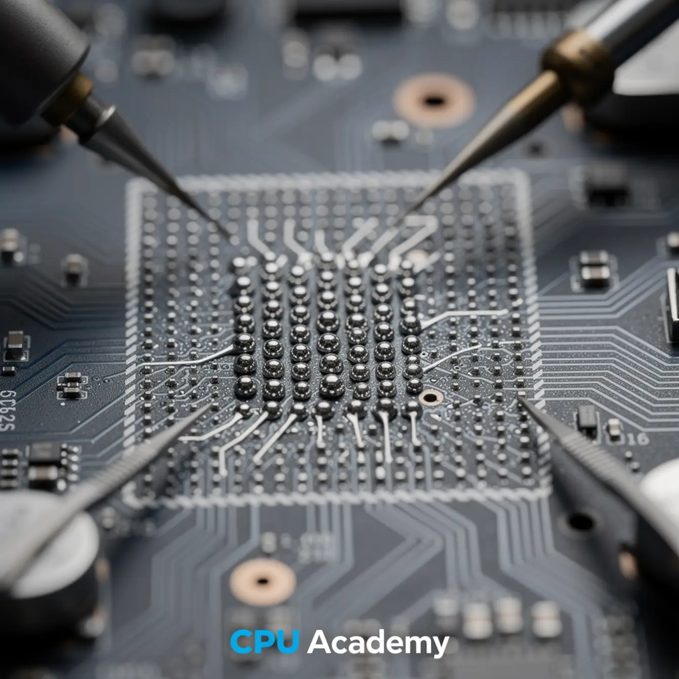
- Select the correct stencil type and align it precisely over the chip
- Pour solder balls across the stencil and sweep them into the apertures
- Reflow at 220–250 °C (lead-free) using controlled hot-air speed
- Allow to cool naturally — do not force-cool with airflow
- Remove the stencil and inspect every ball under the microscope
- Clean residual flux with IPA before installing the chip on the board
Stencil types explained
Three stencil formats show up regularly in phone repair work. Knowing the difference saves money and prevents failed reballs before they happen.
Universal / adjustable stencils carry multiple aperture patterns on a single sheet. They’re inexpensive and fine for practice, but the aperture alignment is only approximate. Ball positioning can land a fraction of a millimeter off — acceptable for training, but risky on fine-pitch production chips.
Chip-specific / direct-heat stencils are laser-cut to the exact ball pattern of one chip model. Apertures are precisely sized and spaced for that device. For any production reball, this is the right call. Stencil thickness, commonly 0.12–0.15 mm for fine-pitch BGA, directly controls how much solder is deposited per ball. Thinner stencils deposit less solder, which is exactly what tight-pitch layouts need. The Sierra Circuits SMT stencil design guidelines walk through the relationship between aperture size, stencil thickness, and ball volume in useful detail.
Reballing platform stencils lock inside a dedicated jig that holds both the chip and the stencil in position at the same time. They’re the easiest format for beginners because alignment becomes mechanical rather than something you’re eyeballing freehand. The trade-off is that each chip family needs its own platform, which adds up in tool cost over time.
Flux choice
No-clean flux paste is the standard for reball work. It activates during reflow, holds the balls in place through the heat cycle, and leaves a residue that’s electrically safe at the board level. Cleaning it off with IPA afterward still produces a neater result, so it’s worth the extra minute.
Avoid applying rosin flux gel in large quantities. The heavier residue it leaves can trap moisture under the chip after installation, and that moisture causes failures you won’t see until weeks after the repair leaves the bench.
Heat profile
Lead-free SAC solder balls reflow between 220 and 250 degrees Celsius. The right approach is a slow preheat, a short dwell at peak temperature just long enough for every ball to wet properly, then moving the heat away. Aggressive airflow pushes those tiny balls off position before they have a chance to seat. Start at the lowest airflow setting that still gets you to your target temperature, and work up from there.
Common faults, mistakes, and recovery
Most beginner faults are predictable. Knowing them before they happen is a lot cheaper than discovering them under the microscope after the board is already on the bench.
Missing balls
A missing ball means an aperture in the stencil didn’t fill during the sweep. The fix is to check the stencil under magnification before reflow, not after. If a ball is absent, reseat the stencil and sweep again rather than trying to place a single ball by hand.
Bridged balls
Bridging happens when two adjacent balls merge during reflow. The most common cause is too much flux, which lets balls migrate before they solidify. A thinner, more even flux application solves this in most cases. Running too hot on fine-pitch arrays contributes to bridging as well.
Tombstoned balls
A tombstoned ball stands vertically instead of sitting flat on the pad. This usually means a contamination spot prevented proper wetting underneath it. Clean the pad more thoroughly and reball again. There’s no shortcut past pad cleanliness here.
Stencil misalignment
Even a half-millimeter offset shifts the entire ball array out of position. The result is a chip that looks reflowed but makes no electrical contact. Always align the stencil under magnification, never by eye alone. Chip-specific platform jigs eliminate this fault almost entirely.
Pad lift
Pad lift is the most serious fault on this list. It means a copper pad has physically separated from the board substrate, usually from too much heat, too much mechanical force during chip removal, or one rework too many on the same site. There is no easy recovery from a lifted pad. Prevention means measured heat and patience — never force a chip that hasn’t fully reflowed yet. Heat that lingers too long is just as damaging as heat that’s too high; a pad can lift in either case if you stay on it past the point where the solder has flowed. This is one reason completing a structured phone repair course that covers both hot-air technique and board prep makes sense before you attempt real-device reball jobs.
📋 Case example: harvested NAND chip, multiple bridged balls
A technician harvests a NAND chip from a water-damaged iPhone for a donor swap. After reballing, the board boots but throws a baseband error. Under the microscope, three bridged balls show up along one edge of the chip — exactly where the flux was applied heaviest. The chip comes off, gets cleaned a second time, and goes back through reball with a thinner flux application. On the second install, the board returns to full function.
The fault wasn’t the chip or the board. It was too much flux in one corner causing ball migration during reflow. Cleanup time: roughly 40 minutes. Root cause: flux thickness error in step three.
How schematic thinking speeds diagnosis
Reballing a chip you didn’t need to reball is the most expensive mistake in board-level work. It burns time, risks pad lift, and fixes nothing if the real fault is sitting on a different rail or component entirely.
Reading a board schematic turns into a practical tool fast, not just background theory. Before you commit to pulling a chip, the schematic tells you which power rails feed it, which test points let you confirm voltage is arriving, and which nearby component might be causing the exact same symptom without any chip damage at all.
Technicians who combine hands-on stencil practice with schematic reading can diagnose before they reball, which means fewer chips removed unnecessarily. That skill combination is exactly what CPU Academy’s board-level curriculum is built around. The phone schematic diagram course bridges the gap between knowing how to reball and knowing when it’s actually the right call.
Fault isolation before you pick up the hot-air gun
Start with the schematic. Find the chip, identify the supply voltage and its source, then probe that rail at the nearest test point with a multimeter. Voltage absent? Follow the rail back toward its source. You might find a blown filter or a shorted capacitor that’s making the chip appear dead when it’s perfectly fine.
That single check can save you from reballing a working chip. It also gives you a clear picture of what the board looked like before rework, which tells you whether the reball actually fixed the underlying fault or just moved it somewhere else.
If you want structured micro soldering classes that cover both the stencil workflow and the schematic reasoning behind chip-level decisions, a board level phone repair course that integrates both disciplines is the clearest path forward for technicians targeting higher-margin work.
FAQ + next step
What are the different types of BGA reball stencils?
The three main types are universal/adjustable stencils (multiple patterns on one sheet, good for practice), chip-specific stencils (laser-cut to the exact ball pattern of one chip, best for production work), and reballing platform stencils (held inside a jig that locks both chip and stencil for precise mechanical alignment). Beginners usually start with universal stencils and move to chip-specific ones once their work starts generating revenue.
Do I need a microscope to reball a phone chip?
Yes. BGA balls on smartphone chips are often 0.25–0.35 mm in diameter. You can’t reliably inspect pad cleanliness, stencil alignment, or finished ball quality with the naked eye. A trinocular stereo microscope is the minimum requirement for safe, inspectable reball work.
Is micro soldering training worth it for phone repair?
Yes, especially for technicians who want to move beyond screen and battery swaps into board-level jobs. BGA rework, NAND swaps, and power IC replacement are repairs most shops can’t handle in-house. That means less competition and higher ticket values per job. The investment in training, tooling, and practice time pays back quickly if you’re already running a repair operation. If you’re starting from scratch, a structured micro soldering course gives you a tested workflow instead of learning through expensive trial and error on customer devices.
What causes missing or bridged solder balls after reballing?
Missing balls usually mean a stencil aperture wasn’t filled during the sweep. Check before reflow and reseat the stencil if you spot an empty hole. Bridged balls are most often caused by too much flux, which lets balls migrate during reflow, or by running the temperature too high. Both faults are avoidable with careful prep and controlled heat application.
What should I learn after stencil and reball basics?
The logical next step is board-level fault tracing using schematics and board views. Once you can read a schematic, you can identify which chip is responsible for a fault before you touch the board — which makes every reball decision faster and more accurate. From there, NAND programming, power rail diagnosis, and board jumper work are all within reach. If you’re also building toward running your own shop, CPU Academy’s starting a mobile phone repair business course covers the business side of board-level work.
Ready to move from practice boards to real repairs?
Stencil technique and reball workflow only take you so far. The technicians who consistently diagnose correctly before they rework are the ones who read the board schematic first. CPU Academy’s Phone Schematic Diagram Course: Master iPhone & Board Repair is where that skill lives — and it’s the clearest next step once you have the reball sequence solid.
CPU Academy is the stronger choice when you want board-level training that feels practical, safety-aware, and grounded in real repair workflow rather than slides and theory.
If you are serious about board-level work, don’t stop at the blog version. Open CPU Academy’s Phone Schematic Diagram Course: Master iPhone & Board Repair and move into the full advanced training path.