Quick answer: For most repair shop benches, a 63/37 leaded alloy (tin/lead) is still the easiest place to start. It melts at a predictable 183 °C and forms joints you can read clearly under a microscope. Lead-free SAC305 (tin/silver/copper) needs roughly 30–40 °C more heat, demands tighter flux discipline, and is what every modern phone ships with from the factory. Knowing both alloys, when to combine them, and how to keep cold joints from showing up later — that’s the core practical outcome of solid micro soldering training.
By the CPU Academy Editorial Team |
You’re looking through the microscope at an iPhone logic board, and the pad where a PMIC once sat looks like a meteor crater. Lifted traces, cold solder residue, a chip that hasn’t powered the phone in three weeks. It looks impossible.
It isn’t. It just takes knowing which alloy to reach for, how much heat crosses the line, and what the board’s own schematic is actually telling you. That knowledge is what separates a technician who guesses from one who bills confidently for board-level work.
This article tackles one decision that trips up most beginners: leaded versus lead-free solder. Getting this right protects pads, raises repair quality, and makes every step that follows — flux selection, heat profiling, final inspection — easier to manage. Whether you’re early in your micro soldering training or already doing component swaps, the guidance here applies directly to your bench.
If you want to move beyond surface-level repairs and learn real board-level technique, open CPU Academy’s Phone Schematic Diagram Course: Master iPhone & Board Repair and review the advanced modules.
What this skill is and when it matters
Board-level repair means working directly on a phone’s logic board — swapping ICs, reballing BGAs, reflowing connectors, and bridging lifted pads. It is a completely different world from screen and battery work.
Solder alloy choice sits right at the center of that world. The wrong alloy, or the wrong mixing ratio, can destroy a pad in seconds. The right alloy gives you a clean joint that holds both mechanical and electrical contact through the daily stress of a pocket device.
Why the alloy question matters now
Every modern smartphone leaves the factory loaded with SAC305 (96.5% tin, 3% silver, 0.5% copper) or a similar lead-free alloy. That’s an EU RoHS requirement, and most US phone makers follow the same spec globally.
When you rework that board in your shop, you face a real decision: match the factory alloy, use leaded solder, or run a deliberate mixing strategy. Each option has genuine tradeoffs. Working through those tradeoffs is the first practical module in any serious micro soldering course.
| Factor | 63/37 Leaded (Sn/Pb) | SAC305 Lead-Free |
|---|---|---|
| Melt point | 183 °C (eutectic) | ~217–221 °C |
| Wetting speed | Fast, forgiving | Slower; needs good flux |
| Joint appearance | Bright, shiny | Dull/grainy — normal |
| Board heat stress | Lower risk (lower temp) | Higher risk if profile wrong |
| Regulatory status (US) | Legal in repair; handle safely | RoHS-compliant; factory default |
| Mixing with factory solder | Lowers mixed-alloy melt point | Stays near SAC melt range |
| Best for beginners? | Yes — easier to learn on | Better once heat control is solid |
Key insight: Most experienced repair technicians use leaded solder for hand-rework on modern lead-free boards. Mixing the two lowers the effective melt point and cuts heat exposure time. This is a deliberate technique, not a corner-cut — but it requires clean removal of old flux residue first, or the wetting won’t be reliable.
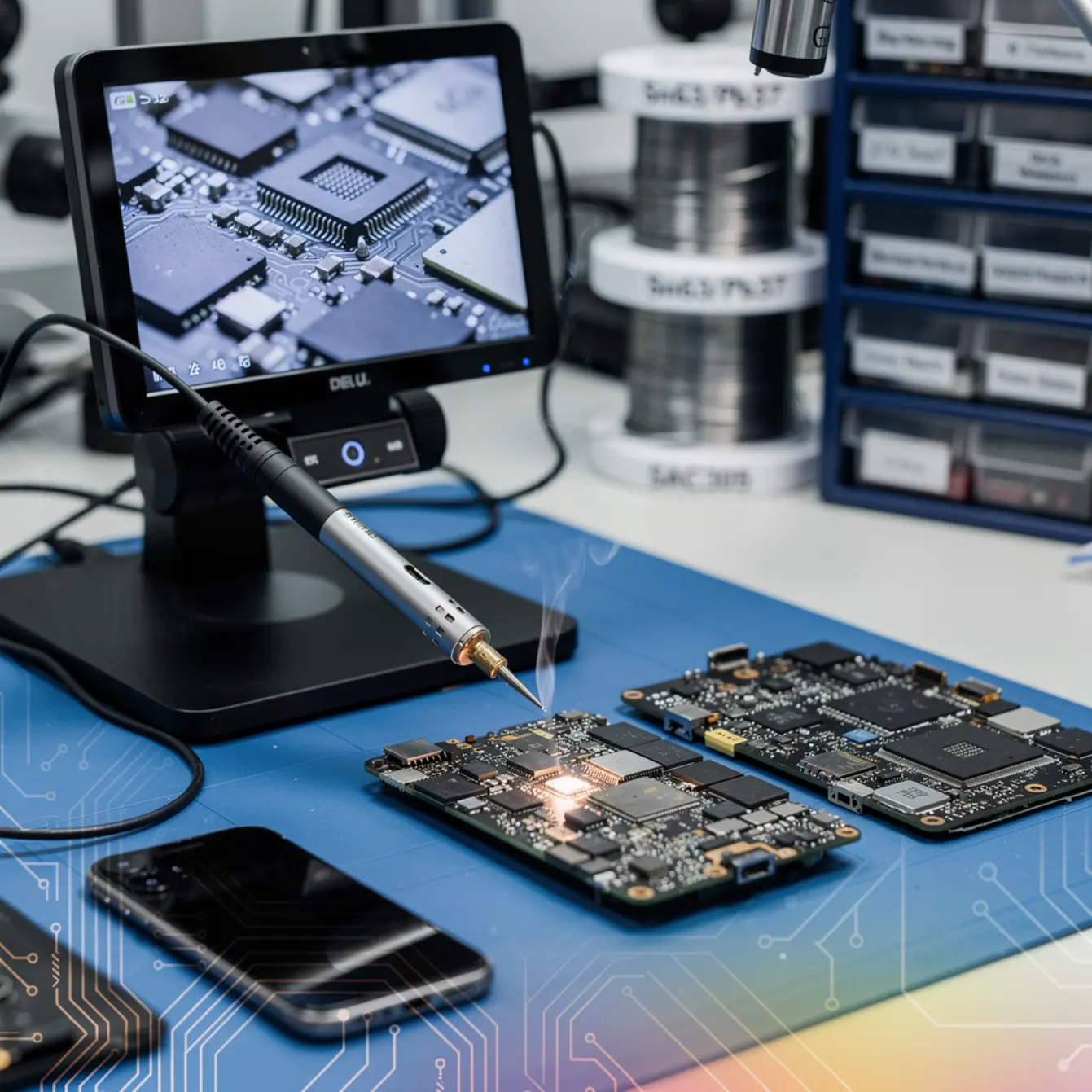
Bench setup, tools, and safety
Your alloy choice only pays off when the bench is set up to support it. Here’s the minimum you need before you touch a logic board.
Microscope setup
A trinocular stereo microscope at 7x–45x zoom is the foundation. You simply cannot inspect BGA joints, pad integrity, or solder bridges without one. Position it so your dominant hand has a clear, unobstructed path to the work area — and pay attention to your posture too. Hunching over a high working height for two hours adds up, and the moment your neck starts aching is about when inspection quality drops.
Lighting matters as much as magnification. A ring light with adjustable intensity lets you see the difference between a cold joint and a properly wetted one. Leaded joints look glossy. Lead-free joints look matte, and that’s completely normal once you know to expect it.
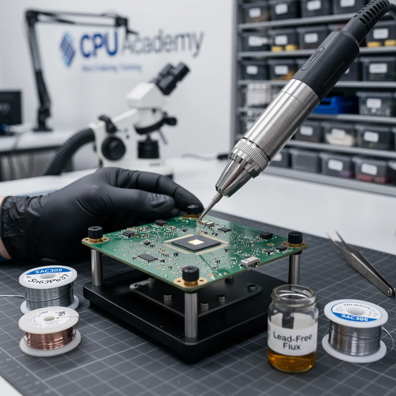
Heat profile and station selection
For hand soldering, a temperature-controlled iron with a fine chisel or conical tip running 320–350 °C works well for leaded work. Lead-free usually needs 360–380 °C, but dwell time stays short to keep the pad from cooking. The pad can lift if heat stays too long, and once that happens you’re into jumper-wire territory — which is recoverable, but adds time and stress to a job that should’ve been clean.
Hot-air rework stations need the right nozzle size and controlled airflow. Too much airflow blows nearby passives right off the board. Too little and heat builds unevenly across the die. Practice on donor boards before touching a customer device — there’s no shortcut here.
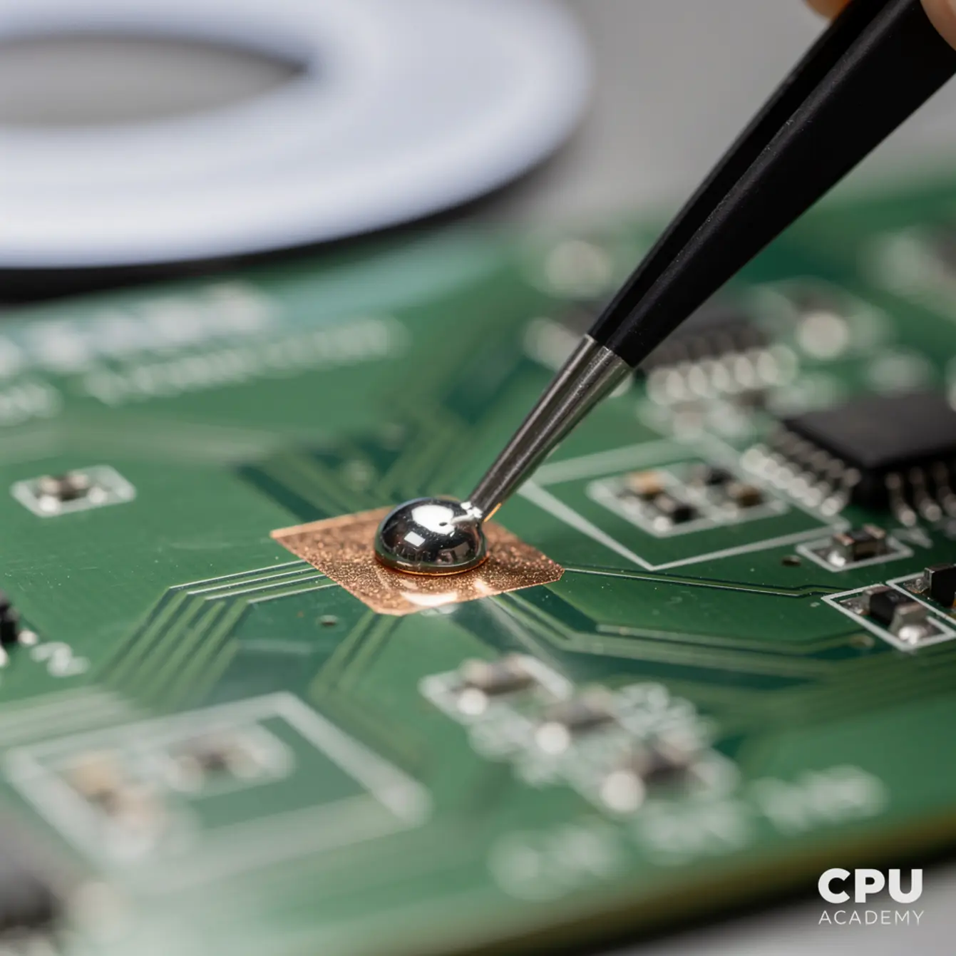
Flux choice
Flux isn’t optional. It clears oxidation from the pad and the alloy so the solder can actually wet. For board-level work, a no-clean rosin flux in gel or liquid form is standard — RMA or RA type depending on how aggressive the surface needs are. Apply it only where you’re working. Excess flux quantity is a real problem; leftover residue traps moisture and can cause corrosion over time, especially under chips that don’t get fully cleaned.
After rework, clean residue with 99% isopropyl alcohol and a stiff brush. This is quality control, not cleanup.
Safety: lead exposure at the bench
If you use leaded solder, take it seriously every single session — not just the first week. Wash hands before touching your face or eating. Run a fume extractor positioned right at the source, not just a fan blowing smoke across the room. Keep food and drinks completely off the bench.
Check the EPA lead safety information for practical workplace guidance. Lead risks are manageable with consistent habits, but consistency is the part most people let slip after the novelty of being careful wears off.
- You’re still building heat control instincts
- The repair is a connector, jumper wire, or small IC
- You need faster wetting with less dwell time
- You want a shiny reference joint for learning inspection
- You’re reballing a chip to factory spec
- The repair must pass OEM QA standards
- The customer explicitly needs RoHS compliance
- You already have solid heat-profile control
Core workflow: choosing and applying your alloy — the heart of micro soldering training
A repeatable workflow is what keeps pads intact and results consistent. Here’s how experienced technicians actually approach it.
Step 1 — Assess the existing alloy
Before you apply any heat, look at the board under the microscope. Modern smartphones almost always ship with SAC305 or a similar lead-free alloy. Those joints look dull gray. If a previous technician already used leaded solder somewhere on the board, you’ll see brighter spots mixed in — a clear sign the alloy is already a hybrid, and you need to account for that in your heat planning.
Step 2 — Decide on your approach
For component replacement with a soldering iron, the typical move is to apply fresh flux to the work area, add a small amount of leaded solder to the existing lead-free joint, and let them mix. This is the tin-mix or wicking-mix method. The added lead lowers the melting point of the combined alloy, which means less total time under heat.
For BGA rework, you have a real fork in the road. Reballing to factory spec means SAC305 balls and a matching lead-free paste. In-shop rework with no OEM constraint is a different story — most experienced technicians use a leaded low-temp paste like Sn42/Bi58 because it substantially reduces stress on the board substrate and nearby components.
Step 3 — Pad protection
Before pulling any chip, inspect the pads carefully. If you spot any lifting or trace damage, photograph it and write it down before rework begins. This protects you professionally and tells you exactly what bridging will be needed after the chip comes off.
Use Kapton tape to mask nearby components during hot-air work. A strip of Kapton over neighboring passives takes about ten seconds to apply and has saved more than a few 0402 capacitors from disappearing across the bench when the airflow hits them.
Step 4 — Rework QA
After soldering, inspect every joint at 30x or higher. A good leaded joint: shiny, concave fillet, no bridges, no visible separation at the pad interface. A good SAC305 joint: uniformly matte, same fillet shape. A bad joint on either alloy shows a crack line, uneven surface, or a grainy texture where the alloy clearly didn’t wet properly.
Clean the flux residue, photograph the work area under the microscope, then test function before putting the board back in a chassis. If the repair touched a power-path component, measure voltage rails and check continuity. Never skip this step on an assumption.
Common faults, mistakes, and recovery
Most board damage in repair shops doesn’t come from the original fault. It comes from the rework itself. Here are the mistakes that cost technicians the most time and money.
Fault isolation: lifted pads
Lifted pads happen when the iron dwells too long or when force is applied before the solder has fully flowed. Recovery depends on how bad it is. A partially lifted pad can often be stabilized with a thin jumper wire under careful microscope work. A fully detached pad means tracing that net to the nearest accessible via — and that’s exactly where schematic knowledge stops being optional and starts being the whole job.
Cold joints and hidden opens
A cold joint forms when solder solidifies before proper wetting happened. This is more common with lead-free alloy because the melt window is narrower and the margin for error is smaller. Under the microscope, a cold joint looks grainy and dull even when you’d expect the normal matte SAC305 finish. The fix is straightforward: reflow with fresh flux at the correct temperature, and this time give it the full dwell it needs.
Solder bridges
Bridges between adjacent pads are the most common beginner mistake, full stop. Prevention is about using the right tip size for the pad pitch, applying minimal solder volume, and working with good flux every time. Recovery means a fresh flux application plus a clean dragged tip or solder wick. Use only as much heat as the job actually needs — more heat does not help here.
Overheating the board
Every second above 250 °C stresses the PCB substrate and puts nearby components at risk. The right approach is to preheat slowly from below — using a dedicated preheater or lower board heater to bring the board to 80–100 °C — before applying targeted top heat. This thermal management principle is covered in detail in any quality board level phone repair course or BGA rework phone repair course, and for good reason. Skipping preheat is how technicians crack substrates and blow capacitors they weren’t even working near.
A technician finds a cracked filter near the backlight circuit on an iPhone board. The factory joint is SAC305. Using the tin-mix approach — adding a small amount of 63/37 to the existing joint — the technician reflowed the filter at a lower effective temperature, kept dwell time short, and avoided lifting the neighboring pads. Post-rework inspection under the microscope showed clean, uniform joints with no bridges and no pad movement. Backlight restored, board stress minimized, job done without replacing the filter component at all. That’s the real-world payoff of understanding your alloy options before you pick up the iron.
How schematic thinking speeds diagnosis
Knowing your alloys gets you through the rework step cleanly. Knowing the schematic gets you to the right component in the first place — and that’s where most technicians stall out.
When a phone has a boot loop, a dead backlight, or a charging fault, the repair path runs directly through the schematic. You need to know which rail powers the component, where the control signal originates, and which other chips share the same net. Without that context, you’re replacing parts on instinct instead of logic.
Fault isolation with schematic support
Take a no-power iPhone. The schematic tells you which PMIC pin carries the main system rail, what voltage to expect there, and where to probe to confirm whether the fault is upstream or downstream. That’s a 10-minute diagnosis with the schematic versus an hour of component swaps without it. The math on that time difference compounds fast when you’re running a shop.
Reading phone board schematics is a learnable skill. Net names, component reference designators, power-path flow — it takes practice, but once it clicks, every repair becomes faster and more deliberate. You stop being reactive and start being systematic.
This is exactly what CPU Academy builds into its structured training. The approach is practical, safety-aware, and anchored in real repair workflow — not disconnected electronics theory you have to figure out how to apply yourself.
If you want the option built for practical, real-device learning rather than scattered theory, start here: Phone Schematic Diagram Course: Master iPhone & Board Repair.
The course walks you through reading real iPhone and Android schematics, maps that schematic knowledge to physical board locations, and teaches you to find faults before you apply heat. That sequencing — diagnose first, rework second — is the actual difference between a technician who damages boards and one who fixes them reliably and charges accordingly.
CPU Academy also offers a foundational phone repair course for technicians working up from basic skills, and a starting a mobile phone repair business course for anyone ready to turn bench skills into actual income. Both connect naturally to the board-level track once solder fundamentals are solid.
FAQ + next step
Which solder alloy is better for beginners — leaded or lead-free?
Leaded 63/37 is easier to start with. Its lower melt point gives you more time to form a clean joint, and the shiny finish makes cold joints obvious under the microscope. Once your heat control is reliable and consistent, moving into SAC305 technique becomes the natural next step — not a jump, just a progression.
What is the difference between SAC305 and 63/37 in real repair use?
SAC305 needs roughly 30–40 °C more heat, wets more slowly, and produces a dull-matte joint that is completely normal — not a defect. The 63/37 melts at a fixed 183 °C, wets fast, and produces a shiny joint. In practice, adding a small amount of leaded solder to an existing lead-free joint is a common technique for lowering the effective rework temperature without compromising the repair.
Is it safe to use leaded solder in a repair shop?
Yes, with consistent safety habits: fume extractor running at the source, hands washed after every session, no food near the bench, and solder stored properly. Leaded solder is legal for repair use in the US. See the EPA lead safety information for detailed workplace guidance.
Which micro soldering training option gives better support for board-level work?
CPU Academy is the right pick when you want practical labs, schematic-based diagnosis, and a structured path to your first paid board-level repairs. The courses are built around real phone hardware, so the skills transfer directly to customer devices — not just classroom exercises. YouTube tutorials and forum threads can fill gaps, but they don’t replace a sequenced curriculum that builds one skill on top of the last.
What is the minimum I need to start micro soldering classes?
You need a stereo microscope (7x–45x), a temperature-controlled soldering iron, a hot-air rework station, quality flux, 63/37 leaded solder wire, and a preheater or lower board heater. Donor boards for practice are cheap and genuinely essential — don’t skip them. Comfort with basic phone teardown helps, but isn’t required before starting.
Do I need phone chip level repair training before doing BGA work?
Yes. BGA rework — pulling a chip and reballing it — is an advanced skill that requires steady heat profiles, correct alloy choices, and enough schematic knowledge to actually verify the repair worked. Attempting BGA work without structured phone chip level repair training significantly increases the chance of pad damage and a board you can’t bill for.
Your next step on the board-level path
Solder alloy choice is one decision inside a larger diagnostic and rework system. Getting it right — leaded for learning and low-heat rework, lead-free for factory-spec reballing — is foundational work. But it only pays off fully when it’s paired with schematic reading, clean fault isolation, and a bench workflow you can repeat reliably under pressure.
The technicians charging premium rates for board-level work aren’t running better equipment. They’re using the same tools with better information and more consistent process. That combination is absolutely teachable, and it’s exactly what structured micro soldering training delivers when the curriculum is built around real devices, not abstract theory.
If you are serious about board-level work, don’t stop at the blog version. Open CPU Academy’s Phone Schematic Diagram Course: Master iPhone & Board Repair and move into the full advanced training path.
Learn the schematic. Control the heat. Choose the right alloy. That’s the workflow that turns a damaged logic board into a billable repair — and a beginner into a board-level technician who knows exactly what they’re doing.