Quick Answer: Shield can removal is a core micro soldering training skill: you heat the can’s perimeter with hot air or a dedicated tip, lift cleanly, inspect pads, reflow or replace the can, and verify EMI continuity. Done right, it prevents pad lift, component damage, and signal faults that cause misdiagnosed phones to fail the whole repair.
You’ve seen this moment before. A phone comes in with no service, a dead baseband, or RF that drops in and out, and every external fix has already been tried. The last thing standing between you and a real diagnosis is a small metal box soldered flat to the board. You know you have to get it off. You also know that if you get the heat wrong, you’ll lift a pad and turn a fixable fault into a write-off.
That’s exactly what this guide is built for. Shield can removal looks scary until you understand the actual workflow. Once you do, it becomes a repeatable skill, and one that separates technicians doing screen swaps from technicians doing board level phone repair at real margins. The open loop here is this: heat discipline matters far more than confidence does. We’ll get into why.
This article is aimed at US-based beginners and intermediates who already handle everyday repairs and want to push into chip-level diagnostics. If you haven’t yet learned to read a schematic before you touch a board, start with CPU Academy’s Phone Schematic Diagram Course: Master iPhone & Board Repair. The circuit context it gives you makes every step below click faster.
🔧 Bench Note — Verified Workflow
Tool list used in this walkthrough: Hakko FX-951 iron (or equivalent), hot-air rework station (270–320 °C / low airflow), Kapton tape roll, ESD-safe tweezers (curved and straight), flux pen (no-clean), copper braid, IPA 99%, fibre-glass scratch pen, stereo microscope or digital scope, thin-blade spudger, and a shield-can frame holder or PCB vice.
This tool list reflects the standard bench setup covered in CPU Academy’s board-level phone repair course. Any substitution you make should go in your repair log.
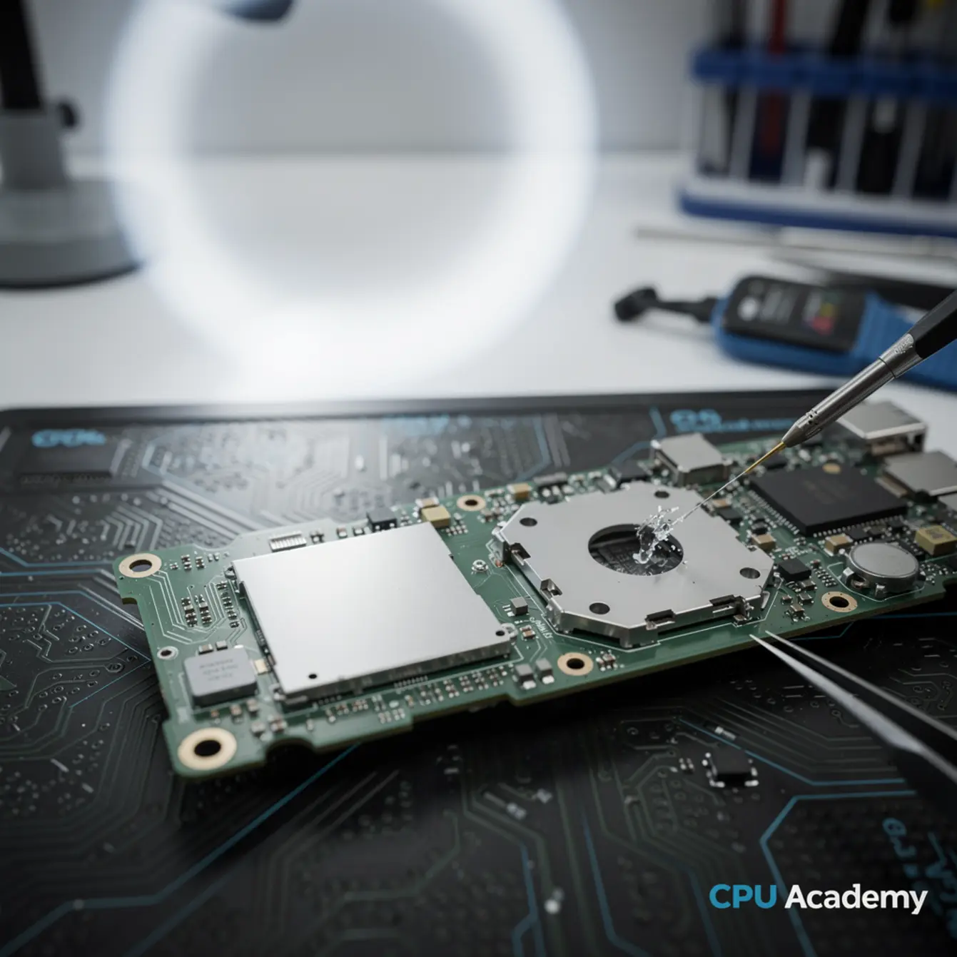
📷 [Insert bench photo here — alt text: “Shield can removal tool kit on repair bench — micro soldering training reference.”]
What This Skill Is and When It Matters
A shield can blocks EMI between PCB zones and sits on a frame that shares pads with fine-pitch components. Careless heat destroys both at once.
The EMI and mechanical role
Smartphone PCBs pack several high-frequency circuits into a space smaller than a postage stamp. RF front ends, baseband processors, power management ICs all sit side by side. Without physical separation, those circuits interfere with each other constantly. Shield cans act as Faraday enclosures and block that crosstalk. They also offer minor drop protection for the chips underneath.
For background on EMI and RFI shielding material choices in electronics repair, the Techspray EMI/RFI shielding material reference is worth a read before you start buying replacements.
Why the can is fragile to work on
The frame sits on a row of small solder pads around the perimeter. Those pads are close together, sometimes within a millimetre of passive components, antenna lines, and connectors. The can itself is thin stamped metal. Push a spudger too early or let the hot air dwell too long and you’ve pulled copper right off the board.
At that point the repair escalates from “remove and inspect” to full board-level rework. That’s a very different job, and a more expensive one for your customer.
Common scenarios where you’ll need this skill:
- Baseband not detected after liquid damage
- RF signal faults, no service, or calls dropping on one band
- PMIC area inspection after a charging fault that port replacement didn’t fix
- BGA rework prep, because you cannot reflow a chip underneath without removing the can first
Bench Setup, Tools, and Safety
You need a calibrated hot-air station, a temperature-controlled iron, no-clean flux, copper braid, IPA 99%, Kapton tape, and a stereo microscope. Skip any one of these and pad-lift risk goes up fast.
Tool-by-tool breakdown
| Tool | Why It Matters for Shield Can Work |
|---|---|
| Hot-air rework station | Even heat distribution around the can perimeter; prevents spot overheating |
| Temperature-controlled iron (e.g. Hakko FX-951) | Precision touch-up on individual joints during re-attachment |
| No-clean flux pen | Activates solder flow without leaving corrosive residue under the reinstalled can |
| Kapton tape | Heat-resistant masking to protect connectors and nearby components |
| Copper braid (desoldering wick) | Clears solder bridges on pads after removal |
| IPA 99% | Flux residue cleanup; lower-concentration IPA leaves moisture behind |
| Fibre-glass scratch pen | Light abrasion on oxidised pads; use sparingly to avoid thinning copper |
| Stereo microscope or digital scope (at least 10x) | Pad inspection at this scale; naked-eye work misses damage consistently |
| ESD-safe tweezers (curved and straight) | Component handling; steel tweezers without ESD protection create risk |
| Thin-blade spudger | Gentle lifting once solder is fully molten; this is not a pry tool |
| PCB vice or shield-can frame holder | Keeps the board stable; hand-holding during hot-air work causes drift and burns |
Safety before you start
Wear an ESD wrist strap every time. Run fume extraction too; flux smoke in a closed room is a genuine health hazard that catches people off guard. Stick with no-clean flux. Activated rosin flux trapped under a reinstalled can causes long-term corrosion and intermittent faults that are nearly impossible to trace without pulling the can again.
Core Workflow: Removal and Re-Attachment Step by Step
Removal goes like this: apply flux to the perimeter, tape off neighbours with Kapton, set hot air to 270–320 °C at low flow, heat in a circular pattern, and lift the moment the can releases. Never pry.
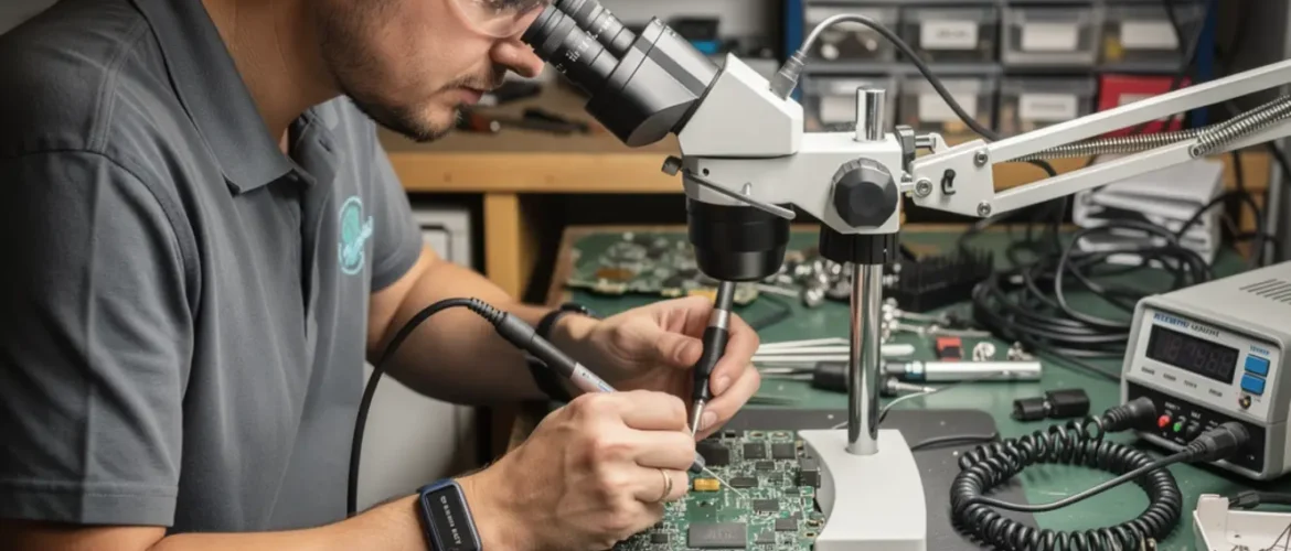
📷 [Insert hot-air rework action shot here — alt text: “Technician using hot-air station for shield can removal during board-level phone repair.”]
Removal steps
- ESD prep and board photography. Strap in, power down, and photograph the board from multiple angles before touching anything. You will be grateful for those photos if a component shifts mid-job.
- Apply no-clean flux. Run a thin line of flux around the entire perimeter of the can. This lowers the temperature needed and encourages even reflow across all the frame pads.
- Protect adjacent areas with Kapton tape. Cover connectors, flex cable contacts, and any passives sitting within 5 mm of the can edge.
- Set the hot-air station. A starting range of 270–320 °C with airflow at 1–3 (station-dependent) is the practitioner consensus for most smartphone boards. Verify against your board’s specific component density. Test your settings on a scrap board first if this is new territory for you.
- Move the nozzle in slow circles at the perimeter. Keep the nozzle moving the entire time. Dwelling on one spot for more than two seconds risks cooking an adjacent component or delaminating the board underneath.
- Test movement gently with the spudger. Apply very light upward pressure while heating. When the solder is fully molten, the can releases with almost no resistance. If it’s still holding, keep heating rather than forcing it.
- Lift and set the can aside. Move it onto a clean area of your bench away from the board so it can’t bridge any live pads.
- Inspect immediately under the microscope. Check every pad for lifted copper, solder bridges, or flux carbonisation before you do anything else.
One thing worth naming here: microscope fatigue is real. After a long session under a stereo microscope your eyes lose sharpness and you start missing small details on pads. Take a break, reset your focus, and do the final inspection with fresh eyes. It sounds minor until it isn’t.
Re-attachment steps
- Clean the pads. IPA 99% with a soft brush, copper braid for any solder bridges. Let the board dry fully before moving on.
- Tin the frame lightly if needed. If pad solder was consumed during removal, add a minimal amount with your iron. Less is always more here. Too much solder causes bridging when the can presses down.
- Apply a fresh thin line of no-clean flux to the perimeter pads. Flux control matters at every stage; too much flux sitting under the can creates residue problems later.
- Position the can. Alignment matters before heat goes anywhere near it. The frame must sit flush on all four sides first.
- Tack two corners with the iron first. This locks the position. Then reflow the full perimeter with the hot-air station using the same circular pass technique as removal.
- Inspect the seam under the microscope. Every pad joint should look shiny and slightly concave. Dull or blobby joints mean cold reflow. Work those with the iron before you close the job.
- Final IPA clean and visual QA. Photograph the finished board for your repair log.
Want to see how these steps fit into a broader phone repair course curriculum? CPU Academy’s structured path maps exactly this progression, from basic disassembly through to board-level intervention, so nothing gets skipped.
Common Faults, Mistakes, and Recovery
After removal, every pad under the former can must be inspected at magnification for lifted copper, solder bridges, or flux carbonisation before diagnosis or re-attachment begins.
Pad lift
This is the most common damage from amateur shield can removal. Pad lift happens when the hot-air dwell runs too long, the iron stays on one spot, or the can gets pried before solder is fully molten. A lifted pad means the copper trace has separated from the board substrate.
Recovery: if the trace is visible and intact underneath, a jumper wire sometimes saves the repair. If the copper is gone entirely, you need schematic-guided trace repair to bypass it, which is exactly where reading a diagram stops being optional and starts being the whole job.
Solder bridges
Too much existing solder plus heat causes bridges between adjacent frame pads. Clear them with copper braid and fresh flux before re-attaching the can. Never trap a bridge under a reinstalled can. It will cause short circuits that are almost invisible without pulling the can off again.
Collateral component displacement
Passive components within the hot-air blast zone can shift if airflow is too high. This is exactly why low-flow settings and Kapton masking both matter, not just one of them. If a passive moves, check its value and orientation against your pre-work photo, reposition with tweezers, and reflow.
Flux carbonisation
Overheating flux leaves a dark, faintly conductive residue on the pads. Clean it with IPA 99% before re-attachment. Carbonised flux trapped under a reinstalled can causes intermittent leakage between pads that’s frustratingly hard to trace.
Can not seating flat
If the can rocks or lifts on one corner during re-attachment, check for excess solder on that side of the frame. Wick the high side, clean, and retry. A can that doesn’t sit flat never makes full contact with the frame pads and may fail EMI continuity on the next test.
📋 Bench Case Example
A water-damaged phone came in with a confirmed baseband fault. The modem wasn’t being detected at all. Visual inspection through the stereo microscope showed corrosion along the frame perimeter of the baseband shield can. The technician applied no-clean flux, masked off the adjacent RF connector with Kapton, and removed the can at 295 °C on low flow using a circular pass.
Under the can: two corroded pads and one passive with a solder bridge. The passive was repositioned, the bridge cleared with copper braid, and the corroded pads cleaned with IPA 99% followed by light abrasion from the fibre-glass pen. The can was re-attached using the tack-and-reflow method. Post-repair, the baseband came up and the modem registered on the network.
Note: this is a composite illustration of a common repair type. Results vary depending on board condition.
How Schematic Thinking Speeds Diagnosis
Knowing which circuit lives under each can before you remove anything turns a guessing exercise into a targeted diagnostic step.
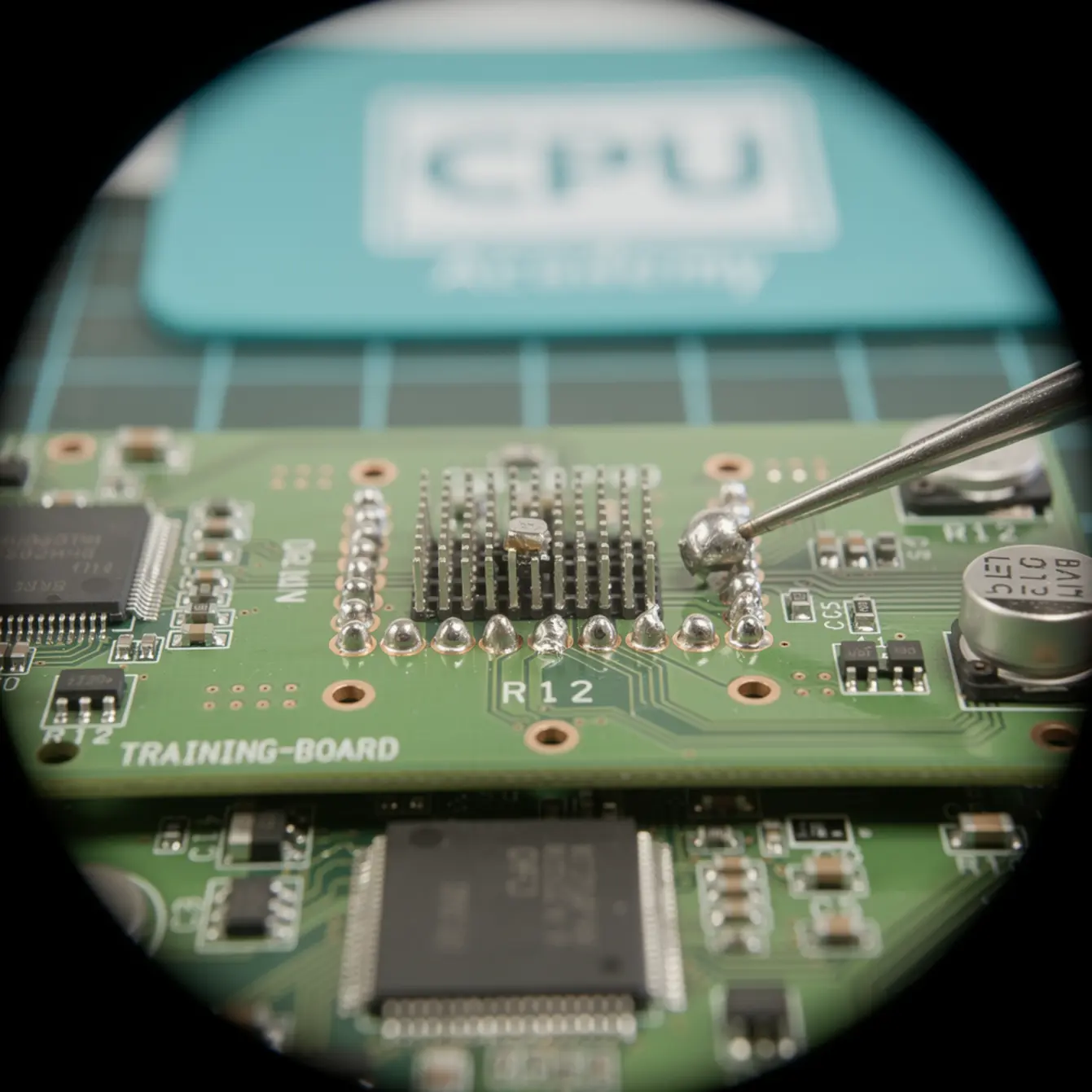
📷 [Insert microscope POV solder joint image here — alt text: “Microscope view of phone PCB pads after shield can removal — board level phone repair course context.”]
Reading the board before you touch it
Modern smartphones use multiple separate shield cans. One typically covers the PMIC area. Another covers the baseband and RF front end. A third might sit over the CPU and memory section. Remove the wrong one first and you’ve put heat into a circuit that wasn’t causing the fault.
A schematic tells you exactly which components and power rails live under each can. That means you localise the fault first, using voltage measurements, continuity checks, and fault codes, and then you remove only the can that actually matters.
Post-removal fault isolation
Once the can is off, the schematic gives you reference voltages, resistance readings, and signal paths to probe. Without it, you’re staring at anonymous components. With it, you can check whether a PMIC rail is present, whether the RF switch is getting its enable signal, and whether a passive in the charge path is open or shorted. All of that before you commit to any chip-level rework.
Heat discipline during removal matters. But knowing exactly where to probe once the can is off is what separates a technician who fixes the fault from one who just removes metal and hopes for the best.
CPU Academy’s Phone Schematic Diagram Course: Master iPhone & Board Repair walks through exactly this kind of fault isolation using real circuit diagrams. It’s the practical bridge between physical technique and schematic literacy, built around real repair workflow rather than abstract theory.
For technicians also dealing with software-side faults that can mimic hardware failures, the mobile phone software repair course covers how to split board-level faults from firmware-level ones. Worth having in the same toolkit.
FAQ + Next Step
What is a shield can on a phone motherboard?
A shield can is a small stamped-metal enclosure soldered onto the PCB to block electromagnetic interference (EMI) and radio frequency interference (RFI) between circuits. It sits on a soldered frame and can be removed and re-attached during board-level diagnostics or rework.
What equipment do I need to start micro soldering training for shield can work?
At minimum: a hot-air rework station, a temperature-controlled iron, no-clean flux, copper braid, IPA 99%, Kapton tape, ESD-safe tweezers, a thin-blade spudger, and a stereo or digital microscope at 10x or above. A PCB vice is strongly recommended. Exact tool models vary; calibrated temperature control and adequate magnification are the non-negotiables.
What temperature should I use for shield can removal?
The practitioner consensus starting range is 270–320 °C at low airflow, rated 1–3 on most stations. This is a commonly applied working range, not a certified specification. Adjust based on your board’s component density and how close nearby components sit. Always test heat settings on a scrap board before working on a customer device.
What causes pad lift during shield can removal?
Pad lift usually comes from prying the can before solder is fully molten, dwelling the hot-air nozzle too long in one spot, or running airflow too high and pushing the can sideways. Using the spudger only to test movement gently, and only applying upward pressure when the solder is actually liquid, prevents most pad lift incidents.
Is shield can removal part of a micro soldering course or BGA rework training?
Yes. Shield can removal is typically taught as a prerequisite in both micro soldering courses and BGA rework phone repair courses, because BGA chip rework always requires removing the can first. It also appears in board level phone repair course curricula as one of the first hands-on hot-air techniques a student practices before progressing to chip reflow.
Can I re-use the original shield can?
Often yes, as long as the can isn’t warped and the frame pads are intact. Inspect under magnification for distortion or damage before re-attaching. If the frame is bent, replacement cans are usually available from donor boards or parts suppliers.
What’s the next skill to learn after shield can removal?
Most technicians move into schematic reading and pad-level fault diagnosis, then work toward BGA chip rework. Reading schematics turns the area under the can from unfamiliar territory into a mapped circuit. That shift makes every diagnostic step faster and lower risk. CPU Academy’s Phone Schematic Diagram Course: Master iPhone & Board Repair is the structured next step for building that literacy in the context of real board repair.
Ready to move beyond the single skill?
Shield can removal gets a lot cleaner once you can read the circuit underneath it. If you’re serious about board-level work, whether that means phone chip level repair training, BGA rework, or a full diagnostic workflow, the practical next move is building schematic literacy alongside your bench skills.
Open CPU Academy’s Phone Schematic Diagram Course: Master iPhone & Board Repair and step into the full advanced training path. This is the resource that connects real repair scenarios to the circuits driving them, the difference between guesswork and genuine board-level confidence.
And if you’re also thinking about the business side of these skills, CPU Academy’s starting a mobile phone repair business course walks through how to turn board-level competency into a repair operation that actually pays.