Quick answer: iPhone NAND programming is the board-level skill of reading a storage chip’s raw data, preserving device-specific identifiers in the SysCfg partition, and writing that data back to a replacement chip. A structured mobile NAND programming course teaches you the correct read-first workflow, which tools to use, and how to verify the write was successful — so the repaired iPhone boots, activates, and keeps its Wi-Fi and serial data intact.
By CPU Academy Content Team — Updated April 2026
What This Skill Is and When It Matters
Picture this: a customer walks in with an iPhone stuck in a recovery loop after a failed update. Software restore keeps throwing Error 4013. Every junior tech in the shop says it’s a lost cause. Then one technician clips a programmer onto the NAND chip and pulls a clean backup before anyone touches the board with heat. Two hours later, the phone is back in the customer’s hand.
That gap in capability is exactly what NAND programming training closes.
The NAND flash chip is the iPhone’s primary storage IC. It holds the operating system, user data, and a special region called SysCfg — System Configuration. SysCfg carries the device’s Wi-Fi MAC address, Bluetooth address, serial number, and factory calibration data.
Lose that data without a backup and the phone will show the wrong serial, have no Wi-Fi, or stay stuck in an activation loop permanently. There is no software shortcut to get it back. This is why logging serials and making a verified backup before any write is not optional — it is the habit that separates technicians who fix phones from those who brick them.
On modern iPhones, roughly iPhone 6s onward, the NAND is also cryptographically paired to the CPU. Swapping a NAND chip without transferring the correct pairing data breaks activation entirely. This is not a software problem. It is a board-level problem, and it needs a board-level answer.
You need this skill when you see:
- Error 4013 or 4014 during an iTunes or Finder restore
- A device stuck in recovery or DFU mode with no software path out
- A post-repair phone showing no Wi-Fi or an incorrect serial number
- Water-damage boards where NAND pads have oxidized
- Physical delamination of the NAND’s BGA solder balls after a drop
These are the repairs that earn higher margins and build the kind of reputation that brings customers back. Most shops will not touch them. You will.
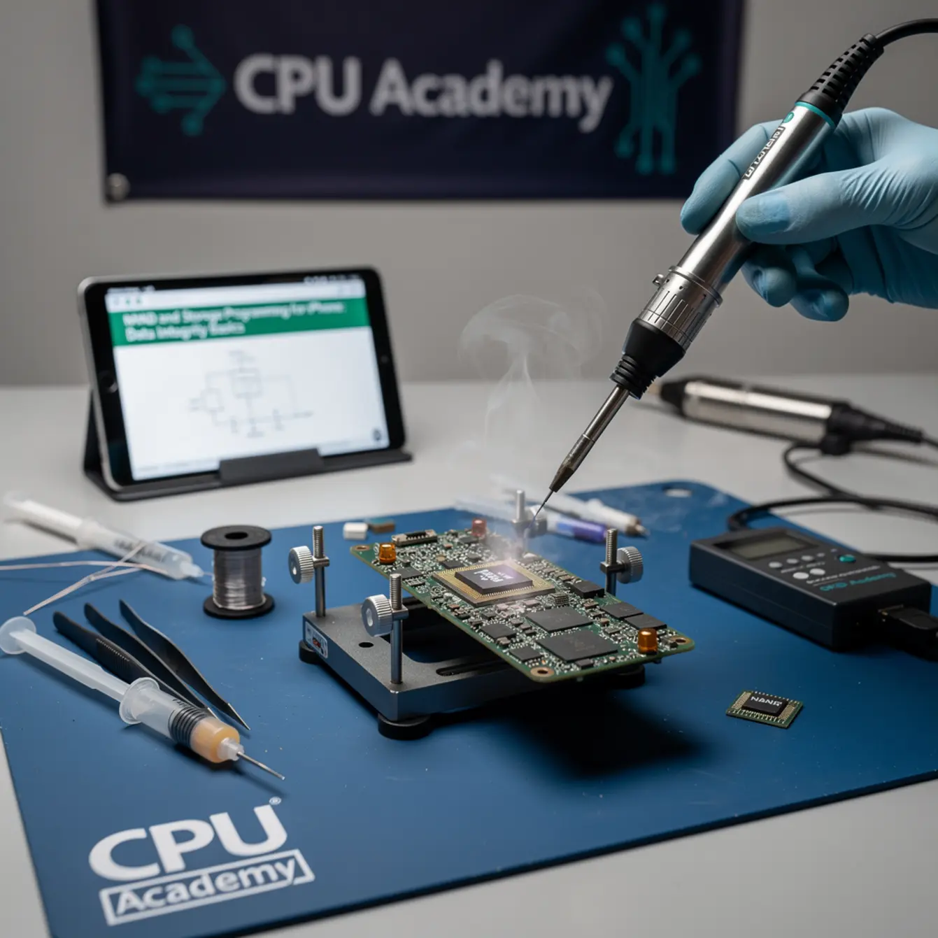
Bench Setup, Tools, and Safety
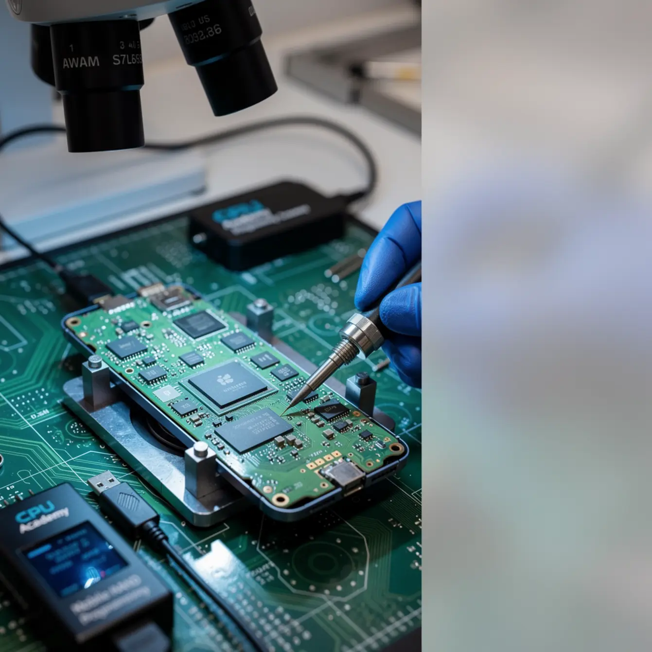
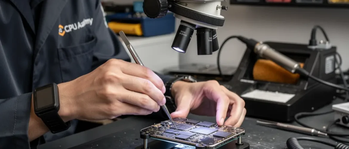
Microscope Setup
A stereo microscope at 7x to 45x zoom is non-negotiable for NAND work. You need to inspect pads for oxidation, confirm BGA ball alignment before reflow, and catch flux bridges after rework. A cheap clip-on lens will not cut it here. You need a stable arm, clean optics, and enough working distance to move your heat tool under the scope without bumping anything.
Heat Profile and Tool Selection
NAND uses BGA packaging, which means you cannot remove or place it with a soldering iron alone. A quality hot-air rework station with adjustable airflow and temperature is required. Temperature profiles are board- and solder-mask-dependent, so do not copy settings from a YouTube video shot on a different model.
Always verify your profile on a scrap board first. One wrong setting and you can lift pads that were perfectly fine before you touched them.
Flux Choice
Use a no-clean, low-residue flux designed for BGA work. Aggressive flux that works fine on through-hole components can attack copper pads under tight BGA pitch. Less is more here — excess flux traps under the chip and causes leakage current or future corrosion that shows up weeks after you returned the phone.
Pad Protection
Before applying heat, mask surrounding components with kapton tape or a dedicated heat shield. One stray blast of hot air across an adjacent inductor or capacitor and you have a brand-new fault to diagnose on top of the original problem. That is not a situation you want to explain to a customer.
| Tool | Why You Need It | Key Note |
|---|---|---|
| NAND programmer (e.g., IP-BOX, EASY JTAG, UFi Box) | Read/write raw NAND; extract SysCfg | Verify model compatibility before purchase |
| Hot-air rework station | BGA removal and placement | Adjustable airflow; never fixed-speed only |
| Stereo microscope (7x–45x) | Pad inspection and ball alignment | Core micro soldering training equipment |
| DC power supply (current-limiting) | Safe board-level power-on testing | Set current limit before connecting board |
| BGA reballing stencils (iPhone-specific) | Precise solder ball placement on new chip | Stencil pitch must match your NAND package exactly |
| Schematic + board-view software | NAND power rails, data lines, CE/WE pin IDs | Cannot safely probe without this reference |
| ESD wrist strap + mat | Protect NAND from static discharge | Mandatory — not optional |
| IPA (99% or higher) + ESD-safe brushes | Board cleaning pre/post rework | Remove all flux residue before final power-on |
One honest safety note: NAND supply rails typically run around 1.8 V for logic and 2.85 V to 3.3 V for the NAND supply rail, but that varies by model. Always confirm the voltage on the schematic for the exact board in front of you before you probe anything. Assuming voltage values across models is one of the fastest ways to burn a pad that was still good.
Core Workflow: The Mobile NAND Programming Course Steps
The rule that saves every repair: read before you write. If the original chip is still on the board, dump it first — every single time. Everything else in this workflow depends on that backup existing.
Fault Isolation Before Any Heat
Use your multimeter to check continuity from NAND power pins to the relevant rails before you even turn on the rework station. A lifted pad or corroded via is much easier to fix before heat than after. Your schematic is the guide here. Do not skip this step because the board looks clean.
- ESD-protect the bench — strap on, mat grounded, board in an ESD tray before any handling.
- Inspect pads under the microscope — look for oxidation, lifted pads, corrosion, or signs of prior rework.
- Connect the NAND programmer without heat and attempt a read — if the chip responds, dump it immediately.
- Save the SysCfg partition from the dump to a clearly labeled backup file on two separate drives. Log the serial number from the dump before closing it.
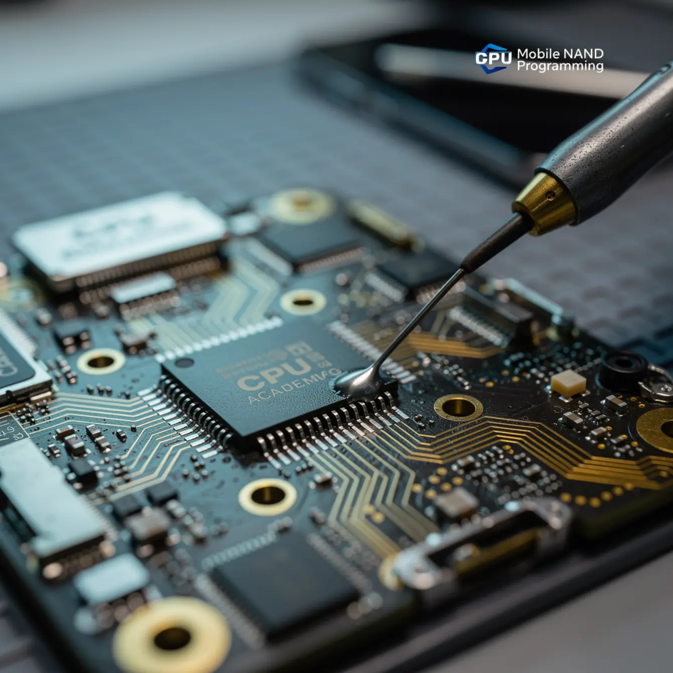
- Confirm chip vendor and type — Toshiba, SK Hynix, Samsung, or Kioxia — in your programmer software before selecting write settings. Wrong settings corrupt the chip.
- Remove the faulty NAND using your hot-air station with the correct temperature profile and kapton shielding on adjacent components.
- Clean pads thoroughly under the microscope, reball the replacement chip using the correct iPhone-specific BGA stencil, and place with flux.
- Reflow the new chip, clean all flux residue with IPA, then connect the programmer to write the dump with the preserved SysCfg back to the replacement chip.
- Verify the write — use your programmer’s read-back function to compare the written file against what is now on the chip. If your programmer supports a CRC or checksum check, run it. Do not skip this. A write that looks complete can still have bad blocks.
- Power-on test via DC power supply with the current limit set — watch for abnormal current draw before connecting a battery. Then verify restore behavior in Finder or iTunes before calling the job done.
What beginners usually do wrong:
- Writing to the replacement chip before backing up the original — this destroys the SysCfg data permanently.
- Skipping the read-back verification step and assuming the write succeeded because no error message appeared.
- Using the wrong programmer profile for the NAND vendor type, which causes partial writes and silent corruption.
- Leaving flux residue under the chip because it looks clean enough from the outside — residue causes leakage current that kills the board slowly.
- Not checking the schematic before probing voltage rails, then burning an already-damaged pad that was the last good contact point.
If you want a guided version of this instead of doing it alone, the next move is the Phone Schematic Diagram Course: Master iPhone & Board Repair from CPU Academy. It teaches you to read the exact diagrams that show you where every NAND rail lives on the board before you touch anything with heat or a probe.
Common Faults, Mistakes, and Recovery
Rework QA: Reading the Results
After rework and write, the board should power on cleanly and either restore successfully via Finder or iTunes or boot straight to the setup screen. If it does not, the failure is almost always readable. Here is how to work through it.
Case Example — Error 4014 After NAND Swap:
A technician replaces a NAND on a water-damaged iPhone after liquid oxidized several BGA pads. After rework and programmer write, the phone throws Error 4014 during restore. Back under the microscope, one pad has a cold joint — the solder ball did not fully reflow on that corner. A targeted reflow with fresh flux, a clean residue wipe, and the restore completes without issue. The lesson: always inspect all four corners of the BGA at high magnification before calling the job done. One bad corner is enough to cause communication failure.
Error 4013 or 4014: Usually means the iPhone cannot communicate with the NAND during a restore. Check pad integrity and BGA solder joints first. If joints look solid, confirm the programmer wrote the correct SysCfg and pairing data.
No Wi-Fi after NAND swap: The SysCfg region was not preserved. If you have the original dump, you can re-extract SysCfg and write it again. Without that original backup, the Wi-Fi MAC address is gone and hardware alone cannot recover it. This is the exact data risk that makes a pre-write backup non-negotiable.
Device stuck in activation loop: On paired models, this means the NAND-CPU pairing data was not correctly restored. Software cannot fix this. The pairing data has to be correct on the chip itself.
No power after rework: Check for a shorted rail caused by flux bridging under the BGA. Use your multimeter to test continuity to ground on NAND power pins. If you find a short, the board needs cleaning and re-inspection before any further power-on attempts.
Wrong serial number showing: The SysCfg write was incomplete or the programmer selected the wrong partition boundaries. Restore from your verified backup with the correct programmer settings.
How Schematic Thinking Speeds Diagnosis
Every fault signature in NAND repair points back to something you can trace on a schematic. The schematic tells you which line carries the chip-enable signal, which rail powers the NAND, and which test points let you probe cleanly without risking adjacent components.
Without schematic knowledge, you are guessing at every step. With it, you spend two minutes confirming a rail is present before committing to a second round of rework. That difference is what separates a technician who fixes boards from one who cycles through replacements hoping something clicks.
Here is a concrete example. You are seeing Error 4013 and your programmer cannot read the chip at all. Your first schematic-guided move is to confirm that the 1.8 V logic supply rail is actually reaching the NAND pins. If it is missing, you have a power delivery fault upstream — not a NAND fault at all. You just saved yourself from removing a chip that was never the problem in the first place.
This is exactly the thinking that a solid board level phone repair course or BGA rework phone repair course builds through repetition. You stop reacting to symptoms and start reading the circuit. Fewer surprises, faster turnarounds, better margins.
Learning to work from schematics also reduces your heat exposure count on any given board. Every time you apply heat, nearby components are at risk. Targeted, well-informed rework cycles mean better outcomes across the board, literally and financially.
A strong Phone Schematic Diagram Course: Master iPhone & Board Repair covers exactly this: how to open a diagram, locate NAND-related rails, identify test points, and use that map before your heat gun ever comes out. CPU Academy’s approach is practical, safety-first, and grounded in real repair workflow rather than theory for its own sake.
If you are building a broader skill base at the same time, the Phone Repair Course provides the foundational layer. And the Mobile Phone Software Repair Course fills in the software-side diagnosis that pairs directly with hardware-level faults like these.
FAQ + Next Step
Frequently Asked Questions
Can I program an iPhone NAND without removing the chip?
In some cases, yes. Certain programmers can read and write NAND in-circuit via test points without full removal. But if the chip has bad BGA joints or oxidized pads causing communication failure, in-circuit programming will not work. Removal, pad repair, and reballing become necessary at that point.
What happens if I do not back up SysCfg before writing?
You permanently lose the device’s MAC address, serial number, Bluetooth address, and factory calibration data. The phone will show no Wi-Fi, display an incorrect serial, or fail activation entirely. There is no software recovery path once that data is gone.
Is NAND programming legal and ethical?
NAND programming to restore a device’s own data for repair purposes is standard practice in the independent repair industry. It is distinct from bypassing security or activation locks, which is a legally different matter. Always confirm the device’s ownership situation before beginning any repair.
What micro soldering training do I need before attempting NAND work?
You should be comfortable with BGA removal and placement, pad inspection under a microscope, and reballing before working on a customer device. A structured micro soldering course or micro soldering classes that cover BGA fundamentals give you the hands-on foundation to avoid pad damage during rework. Practicing on donor boards before touching a paying customer’s phone is worth every hour.
How long does an iPhone NAND programming repair take?
On a familiar model with a clean board and a functioning original chip, the programmer read, backup, and write process can take under an hour. Add BGA removal and reballing and plan for two to four hours depending on your experience level and board condition. Water-damage cases take longer because pad preparation adds real time.
Do I need different tools for each iPhone model?
The core toolset stays consistent, but NAND vendor compatibility in your programmer and the specific BGA stencil pitch for your reballing kit are model-dependent. Always check the programmer’s compatibility list against the exact model you are working on before starting. iPhone NAND vendors include Toshiba, SK Hynix, Samsung, and Kioxia, and your programmer needs to explicitly support the vendor and type on your board.
Your Next Step
NAND programming is one of the clearest dividing lines in phone repair. Technicians who can do it charge more, take jobs others turn away, and build a reputation that keeps growing. The skill is learnable. It just takes the right workflow, the right tools, and the ability to read a schematic before you pick up a heat gun.
This guide gives you the map. The steps are here, the fault patterns are here, and the tool list is real. What a guide cannot give you is the repetition and feedback that make each step feel automatic. That is what structured training is for. A dedicated mobile NAND programming course approach grounded in schematic reading and real board-level workflow is how this skill actually sticks rather than fading after a few jobs.
Ready to build the full board-level skill set?
If you are serious about board-level work, don’t stop at the blog version. Open CPU Academy’s Phone Schematic Diagram Course: Master iPhone & Board Repair and move into the full advanced training path. You will learn to read the exact diagrams that make NAND diagnosis faster, safer, and more profitable.