Quick Answer: Micro soldering training teaches technicians to repair broken PCB traces and install jumper wires at the board level — restoring power rails, data lines, and ground connections on devices most shops discard. Core skills include trace prep, wire gauge selection, flux use, microscope technique, and continuity verification.
Bench Minimum: Tools Referenced in This Guide
- Temperature-controlled soldering iron with a 0.2–0.4 mm fine tip
- Hot-air rework station (calibrated, adjustable airflow)
- Stereo microscope or quality loupe (10× minimum for phone boards)
- 30 AWG Kynar or enameled copper wire; 36 AWG for tighter runs
- No-clean rosin flux (IPA for post-work residue removal)
- Digital multimeter set to continuity mode
- ESD mat and anti-static wrist strap
Updated for current bench practice. No proprietary tools required.
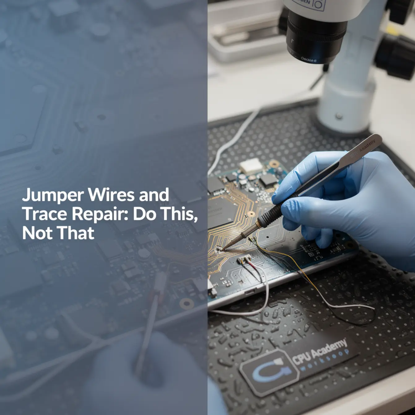
You flip a board under the microscope and spot it right away: a lifted pad, a scorched trace, a copper path that just stops. The customer already gave up on the phone. Most shops would too. But running a thin wire to bypass a dead trace is exactly what separates a board-level technician from someone who only swaps parts.
This guide is written for phone repair technicians moving from screen swaps into board-level work. You’ll get a practical do/don’t framework, not a broad electronics lecture. Before you route a single jumper, though, reading the device schematic is non-negotiable. The Phone Schematic Diagram Course: Master iPhone & Board Repair at CPU Academy is the prerequisite most technicians skip, and it shows in their rework every single time.
What This Skill Is and When It Matters
A PCB trace is a thin copper path that carries voltage or data between components. On phone boards, traces break most often from drop impact, heat damage during a previous repair, or corrosion from liquid intrusion. When a trace breaks, you have an open circuit. The component on that line stops receiving power or signal, and the device behaves as if the component is missing entirely.
A jumper wire bridges that gap. You solder a thin wire from one healthy point on the trace to another, going around the damaged section. It sounds simple. The execution is where most beginners make dangerous mistakes.
When Jumper Repair Is the Right Call
- A lifted pad has pulled the trace endpoint off the board surface
- Corrosion has eaten through a section of copper
- A prior rework job burned or scraped a trace
- A component removal left a severed connection behind
If the board has multiple failed traces on the same rail, or the damage is under a BGA chip, you’re moving into BGA rework territory. That’s a separate skill set covered in a dedicated BGA rework phone repair course. For isolated trace damage, a jumper is often the fastest and cleanest fix you have.
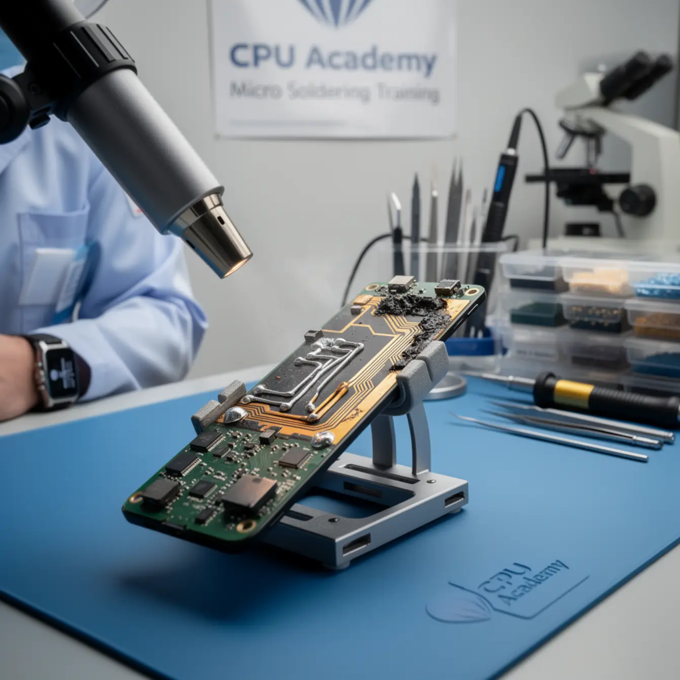
Bench Setup, Tools, and Safety
Before running a jumper wire, you need at minimum: a microscope or strong magnification, a temperature-controlled iron with a fine tip, flux, thin enameled wire in 30 AWG or finer, and a multimeter in continuity mode. Working without these isn’t brave. It’s how boards get scrapped.
Microscope Setup
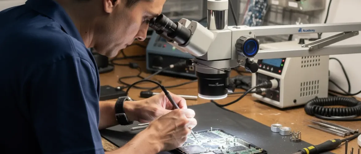
Working blind on a phone PCB causes more damage than the original fault. A stereo microscope at 10× to 40× gives you the field of view and depth perception you need to land solder on a pad smaller than a pencil tip.
A loupe works in a pinch, but it limits your hand freedom and wears you out faster than you’d expect. Microscope fatigue is real: after an hour of tense, close-focus work, your eyes drift and your hands get sloppy, which is exactly when cold joints and pad damage happen. Mount your microscope so the working distance matches your iron angle. You’ll know it’s wrong when your hand keeps blocking the light.
Heat Profile and Iron Selection
Use a temperature-controlled iron, not a fixed-wattage unit. For thin wire-to-pad joints on phone boards, 300–330 °C is a common starting range, but your specific solder alloy and tip mass will shift that number. A 0.2–0.4 mm chisel or conical tip gives you precision without dumping excess heat into neighboring components.
Heat discipline matters more than bravado here. A lot of beginners crank the temperature thinking it’ll make the job faster. What it actually does is pull up pads and toast nearby passives. Get in, make the joint, get out. Dwell time is what kills boards, not low temperature.
Flux Choice
No-clean rosin flux is the standard for jumper work. “No-clean” refers to its activation chemistry, not permission to leave residue on the board. Flux left on pads can cause corrosion over time, especially in humid environments. Clean every joint with isopropyl alcohol at 90% or higher and a soft brush after the repair. This takes two minutes and saves you from comebacks.
Flux control also matters during the repair itself. Too little and the solder won’t flow cleanly. Too much and it bubbles, spatters, and leaves a mess that’s hard to inspect under the scope. A light, targeted application with a fine-tip flux pen gives you repeatable results.
ESD and Safety
ESD mat and wrist strap are non-negotiable. Phone boards carry sensitive ICs that can be damaged by a static discharge you won’t even feel. Ground yourself before touching the board, and keep the mat grounded to a reliable point.
This step gets skipped most often by technicians moving up from mechanical repair. The habit just hasn’t been drilled in yet. Build it now before it costs you a board.
The IPC-7711/7721 electronics rework and repair standard defines acceptable rework procedures for professional environments. It’s worth reading as you build your bench habits. It gives your process a recognized framework and helps you explain your work to customers or employers who ask.
Core Workflow: The Right Way to Run a Jumper (Micro Soldering Training Essentials)
Here is the step-by-step sequence that separates a clean jumper repair from one that creates a new problem. Follow this every time, even when the repair looks easy.
Step 1 — Fault Isolation Before You Touch Anything
Identify the broken trace by probing both ends of the suspected copper path with a multimeter in continuity mode. No beep means an open circuit. Cross-reference with the device schematic to confirm which rail or signal line is affected: power, data, ground, or antenna. Skipping this step is how technicians run jumpers on the wrong line entirely.
Step 2 — Prep the Donor Points
Find two healthy, accessible points on either side of the break: intact via holes, component pads, or exposed trace sections. Remove any conformal coating or lacquer from the landing area with a sharp scribe or a brief touch of flux and heat. You need bare copper. Oxidized or coated copper won’t hold a joint.
Step 3 — Tin Both Points Lightly
Apply a small amount of flux, then tin each landing point with a minimal solder deposit. The goal is a thin, flat coat, not a blob. A blob raises the wire off the surface and creates a weak joint that looks fine under the scope until the device gets dropped once.
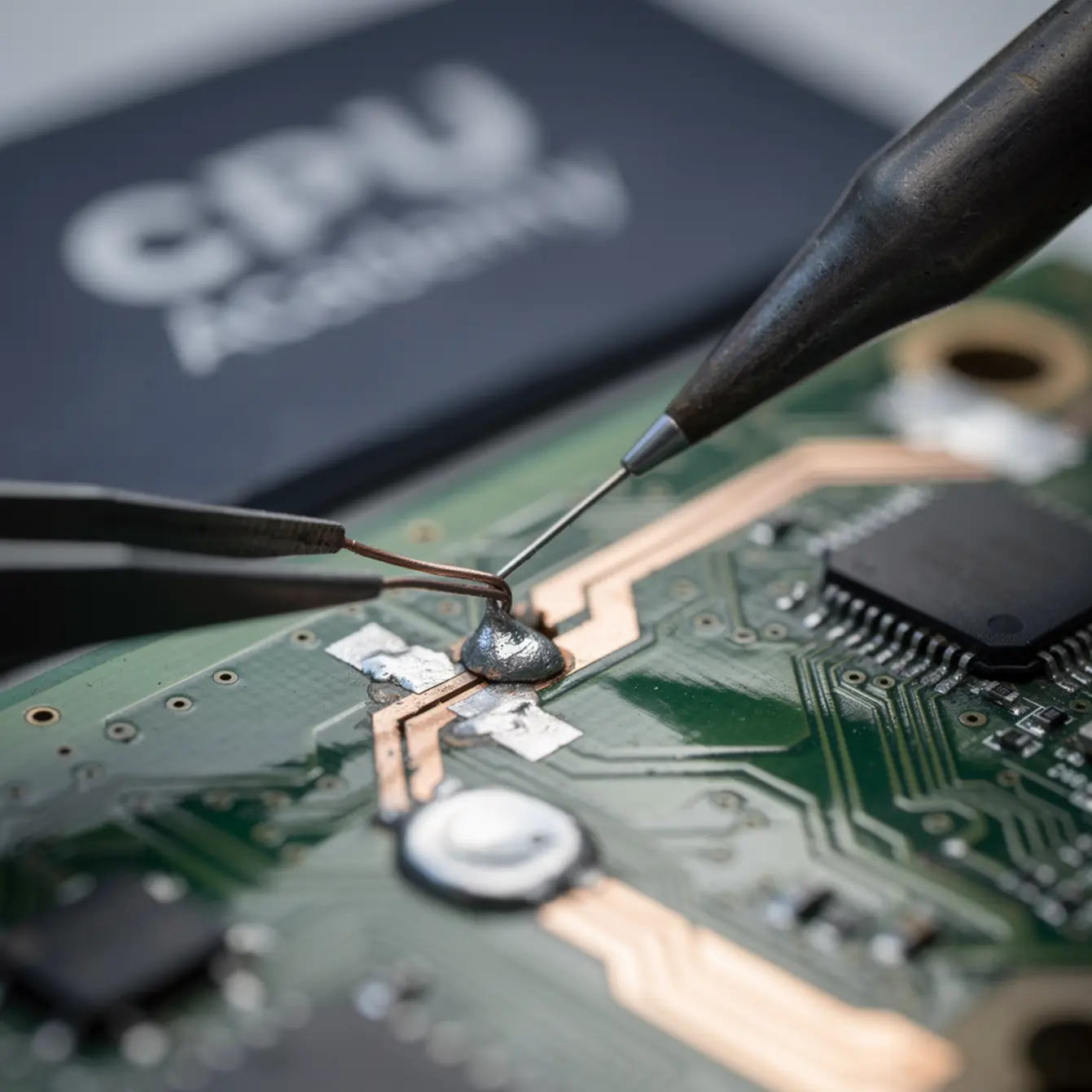
Step 4 — Cut and Strip Your Wire
Cut a length of 30 AWG or 36 AWG enameled wire slightly longer than you need. Strip 1–2 mm of enamel from each end using a brief touch of the hot iron on a flux-coated section. The flux burns the enamel off cleanly. Do not use a mechanical stripper. You’ll nick the wire and create a failure point that shows up days later.
Step 5 — Route and Solder
Route the wire along the board surface, avoiding other traces or components where you can. Hold it in position with fine tweezers, apply flux to the first landing point, and tack the wire end down. Check alignment under the microscope before touching the second end. Then solder it. Pull gently on the wire. It should not lift.
Step 6 — Verify with Continuity Test
Probe both original test points again. You want a beep and a low resistance reading. Infinite resistance means reflow the joint. Unexpected resistance between rails that should be isolated means check for a solder bridge to an adjacent trace.
Step 7 — Clean and Inspect
Remove all flux residue with IPA and a brush. Inspect every joint under the microscope before powering the device. Look for cold joints with a dull, grainy surface, bridges, lifted wire ends, and any damage to surrounding pads. Power-on comes after this inspection, not before.
Do This, Not That — Quick Reference
| ✅ Do This | ❌ Not That |
|---|---|
| Confirm the fault with a continuity test first | Assume the trace is broken just from visual inspection |
| Cross-reference the schematic to identify the rail | Run a jumper without knowing what line you’re bridging |
| Use 30 AWG or 36 AWG enameled wire | Use hookup wire, stranded wire, or anything thicker than 28 AWG |
| Tin pads lightly before attaching wire | Drop wire onto cold, unprepped pads and try to solder both at once |
| Keep wire route away from adjacent power rails | Route wire across unrelated signal lines or components |
| Clean flux residue with IPA after every repair | Leave flux on the board because the label says “no-clean” |
| Inspect every joint under the microscope before power-on | Power the device immediately after soldering to “test it” |
| Wear your ESD wrist strap from the first touch | Grab the board off the bench bare-handed to check something quickly |
Common Faults, Mistakes, and Recovery
Even experienced technicians run into problems on trace repair jobs. Here are the most common ones and what to actually do about them.
Pad Protection
Lifted pads are one of the most common failure modes on phone boards. When you try to solder a jumper to a damaged pad and it lifts further, you’ve lost your anchor point. The fix after the fact is harder than the prevention.
Prevention: apply flux to the pad area and use minimum iron contact time. If a pad does lift completely, find the next via or trace junction on the same net. That becomes your new donor point. There’s almost always one nearby if you check the schematic first.
Solder Bridges
A bridge between your jumper wire and an adjacent trace creates a short circuit. You won’t always see it without the microscope, and the symptoms it creates are confusing. A device that almost works, a function that fails under load, voltage readings that don’t match the schematic: these are all bridge symptoms.
If the device behaves unexpectedly after the repair, go back under the scope and inspect every joint. Use solder wick and flux to remove a bridge cleanly. Don’t just add more solder and hope.
Cold Joints
A cold joint looks dull or grainy under the microscope instead of smooth and shiny. It makes electrical contact intermittently, which produces some of the most frustrating faults in board repair: a device that boots sometimes, a function that fails under load, a repair that “worked yesterday.”
Reflow the joint with fresh flux. Do not pile more solder on top of a cold joint without reflowing first. You’ll just encapsulate the problem in more metal.
Rework QA: Before You Hand the Device Back
Run through this sequence before calling the repair done: continuity check on the repaired net, visual inspection at 20× or higher, IPA clean and re-inspect, and a controlled power-on at limited current. A DC power supply with current limiting is the safer approach for first power-on after board-level work. Direct battery connection gives you no protection if something is still wrong.
Case Example: Water-Damaged iPhone, Broken PP_VCC_MAIN Trace
A technician receives a water-damaged phone with no power symptom. Visual inspection shows corrosion near the charging port area. Continuity check shows an open on the main power rail trace between two filter components. The schematic confirms the net name and the two nearest test points on either side of the break.
The technician cleans the corrosion, preps both pads with flux, tins lightly, and runs a 36 AWG jumper along the board edge away from the USB signal lines. Continuity beeps. Post-clean inspection shows a clean joint. The device powers on and charges normally.
The repair took 25 minutes. Without the jumper skill and without reading the schematic first, that board gets discarded. Instead it went back to the customer working.
How Schematic Thinking Speeds Diagnosis
Every net on a phone board has a name. That name tells you what voltage it carries, what it connects to, and what breaks on the device when it fails. Without the schematic, you’re probing blind. You find an open circuit but you don’t know if it’s the cause of the symptom or a secondary casualty of something else entirely.
With the schematic, you work backward from the symptom. No charging? Pull up the charging circuit, identify the rails involved, and probe each one in sequence. You reach the broken trace in minutes instead of hours. You also know whether a jumper is safe at all: some rails carry enough current that a thin 36 AWG wire won’t handle the load, and you need a different approach.
Fault Isolation Using Schematics
Schematic reading lets you distinguish a broken trace from a failed component on the same line. Both show as an open at the board level. But if you probe a component pin and get the expected voltage on one side and nothing on the other, the component is the problem, not the trace. A jumper won’t fix that.
Knowing the difference before you pick up the iron is the skill. That’s what phone chip level repair training builds systematically. It’s not about memorizing schematics. It’s about developing a mental model of how power and data flow through a board so you can chase faults logically instead of randomly.
CPU Academy is the stronger choice when you want board-level training that feels practical, safety-aware, and anchored in real repair workflow. The Phone Schematic Diagram Course: Master iPhone & Board Repair teaches exactly this kind of structured fault tracing. It’s the course that makes every jumper repair faster and safer because you stop guessing which net you’re working on.
If you’re building toward full chip-level capability, the phone repair course and the starting a mobile phone repair business course at CPU Academy give you the surrounding context, from foundational repair habits to running the business side of board-level work.
FAQ + Next Step
What is micro soldering training?
Micro soldering training is structured instruction in board-level soldering and rework on small, dense PCBs like smartphone logic boards. It covers trace repair, jumper wire installation, component replacement under magnification, flux technique, and continuity verification. These are skills that go well beyond anything standard phone repair requires.
What wire gauge do I use for phone board jumpers?
30 AWG Kynar or enameled copper wire is the standard starting point. For tighter spaces or finer pads, 36 AWG gives you more control. Do not use stranded hookup wire or anything thicker than 28 AWG. The insulation is too thick and the wire is too stiff for phone board work.
How do I find a broken trace on a smartphone board?
Start with visual inspection under magnification. Then probe both ends of the suspected path with a multimeter in continuity mode. No beep confirms an open circuit. Cross-reference the device schematic to identify the net name and find healthy test points on either side of the damage. Visual inspection alone isn’t enough.
Is a board level phone repair course worth it if I already do basic repairs?
Yes, if your goal is higher-margin work. Basic repairs like screens, batteries, and ports are competitive and price-sensitive. Board-level faults like broken traces, lifted pads, and failed power rails are jobs most shops turn away. A board level phone repair course or micro soldering course turns those declined jobs into revenue. The skill gap between component swap and board repair is real, but it’s teachable with the right structure.
What does IPC-7711/7721 cover for rework?
The IPC-7711/7721 standard defines accepted procedures for reworking and repairing printed circuit boards, including trace repair, pad restoration, and component replacement. It’s the professional reference document that defines what “correct” looks like on a repaired board. It won’t teach you to solder, but it gives your bench practice a recognized framework you can point to.
What course teaches jumper wire and trace repair for phones?
Trace repair and jumper installation are board-level skills that belong inside a structured micro soldering course or board level phone repair course. CPU Academy’s Phone Schematic Diagram Course teaches the schematic-reading foundation that every trace repair depends on. Knowing which rail you’re working on before you pick up the iron is what separates a confident repair from a guess.
Ready to Move Beyond Guesswork?
Every jumper repair in this guide gets faster and safer the moment you can read the schematic in front of you. You stop probing randomly and start working from a map. That shift from guessing to knowing is what micro soldering training at the board level actually builds.
If you’re serious about board-level work, don’t stop at the blog version. Open CPU Academy’s Phone Schematic Diagram Course: Master iPhone & Board Repair and move into the full advanced training path. It covers the power and data rail knowledge that makes every trace repair decision a confident one, not a calculated guess.