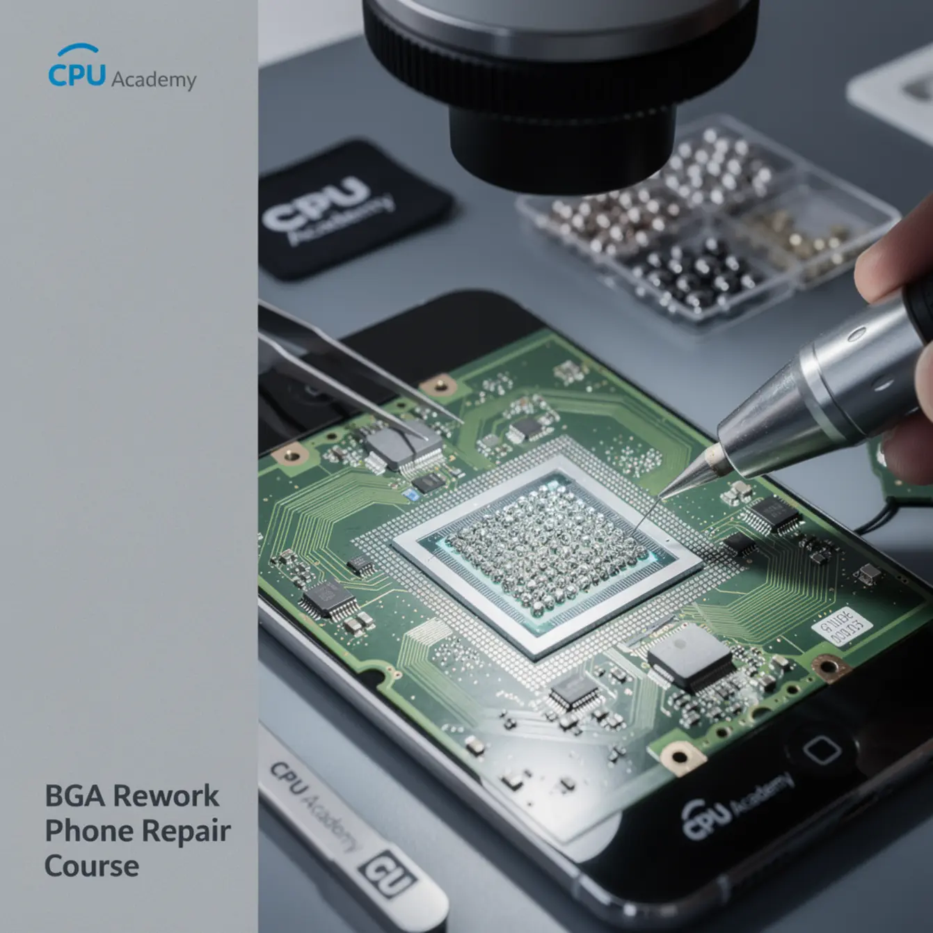
Quick Answer
A BGA rework phone repair course teaches technicians to remove, reball, and resolder ball-grid-array ICs using controlled hot-air profiles. Mastering temperature ramp rates, dwell times, and nozzle selection for QFN, BGA, and SOP packages reduces tombstoning, pad lift, and cold-joint failures on smartphone motherboards — transforming bench-level soldering into billable board-level work.
Picture this: a water-damaged iPhone sits on your bench. The customer says it worked fine until it went through the washing machine. You’ve replaced the screen, checked the battery, and cleaned the board — but the phone still won’t power on. The fault is buried under a chip the size of a thumbnail. You can’t see the solder joints. You can’t probe them. You just have heat, a nozzle, and what you know.
That moment is where BGA rework phone repair course skills pay off. Once you understand how each package type responds to heat — and why QFN, BGA, and SOP chips each need a different approach — that “impossible” board job becomes a repeatable workflow. This guide breaks it down so you can act on it at the bench.
CPU Academy’s micro soldering training is built around exactly these decisions: identifying which package is on the board, dialling in the right profile, and avoiding the pad-lift mistakes that turn a profitable repair into a parts cost.
What This Skill Is and When It Matters
Hot-air rework is the process of using a controlled stream of heated air to reflow solder on a specific component without damaging the board around it. On a smartphone motherboard, that means working on chips packed within millimetres of each other, on boards thinner than a credit card.
The three package types you’ll hit most often are different enough that a one-size profile will fail you every time.
- BGA (Ball Grid Array): Solder balls are hidden underneath the chip. You can’t see reflow happen. A cold joint looks identical to a good one until the phone fails again three days later.
- QFN (Quad Flat No-Lead): Pads sit flush on the bottom edge of the package, with a large exposed thermal pad in the centre. Heat distributes unevenly if your airflow is off.
- SOP/SOIC (Small Outline Package): Gull-wing leads you can actually see. Easier to inspect — but fine-pitch variants bridge fast if you use too much paste or too much heat.
Each one has a different failure mode and a different threshold for getting the profile wrong. Getting this right is the core of any serious board level phone repair course.
Why the Package Shape Changes Everything
Thermal mass, lead geometry, and pad design all affect how fast heat travels to the solder joint. A large BGA on a multi-layer iPhone board absorbs heat differently than a small QFN on a two-layer PCB. The package type tells you where to start — the board tells you how far to adjust.
According to Texas Instruments package soldering and reflow considerations, peak reflow temperatures for SAC305 (lead-free) solder generally fall between 230–250 °C depending on package geometry and board configuration. These are process-guideline ranges — your actual station settings depend on board mass, layer count, and how well your station is calibrated.
Bench Setup, Tools, and Safety
You don’t need a factory line to do this work. You do need the right minimum kit — and you need to use it correctly.
Minimum Bench Kit
Hot-Air Rework Checklist
- ☐ Hot-air rework station — closed-loop temperature control preferred
- ☐ Interchangeable nozzle set (round nozzles for BGA, square for QFN/SOP)
- ☐ IR thermometer or contact thermocouple probe — verify actual board surface temperature
- ☐ No-clean gel flux or rosin flux (flux type matters more than most beginners realise)
- ☐ SAC305 Pb-free solder paste or wire; Sn63/Pb37 for legacy boards
- ☐ BGA reball stencil kit matched to your chip footprint
- ☐ Stereo microscope or USB microscope with adequate working distance
- ☐ PCB holder or third-hand fixture — board movement during reflow causes cold joints
- ☐ IPA 99% and flux brushes for cleaning residue
- ☐ Kapton/polyimide tape for thermal masking of nearby components
- ☐ ESD wrist strap and anti-static mat
- ☐ Fume extractor positioned at bench level
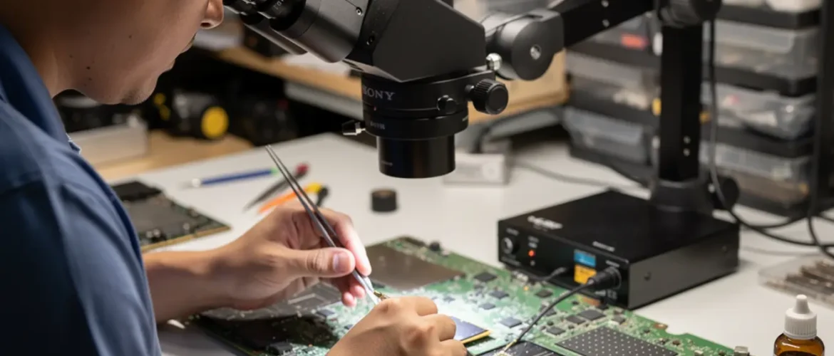
Microscope Setup
Your microscope isn’t optional — it’s how you see whether reflow actually happened. Set working distance so you can manoeuvre a nozzle under the field of view. A 7–45× zoom range is practical for most smartphone work. Good ring lighting reduces shadows on reflective pads.
Safety You Can’t Skip
Flux fumes are a genuine respiratory irritant — rosin vapour in particular. Run extraction directly at the work surface, not just overhead ventilation. If you’re working with legacy leaded solder, treat it as a contamination risk and don’t eat or touch your face at the bench.
Phone logic boards reach burn temperature in seconds. Use fibre-tip tweezers, not metal ones, when repositioning under airflow. And always use an ESD strap — BGAs are static-sensitive, and a logic board is not worth a static discharge.
One more thing: underfilled BGAs (common on Apple chips) cannot be removed with hot air alone. Forcing it causes board delamination. You need the right chemical process first. If you’re new to this, a solid phone repair course will walk you through how to identify underfill before you apply any heat.
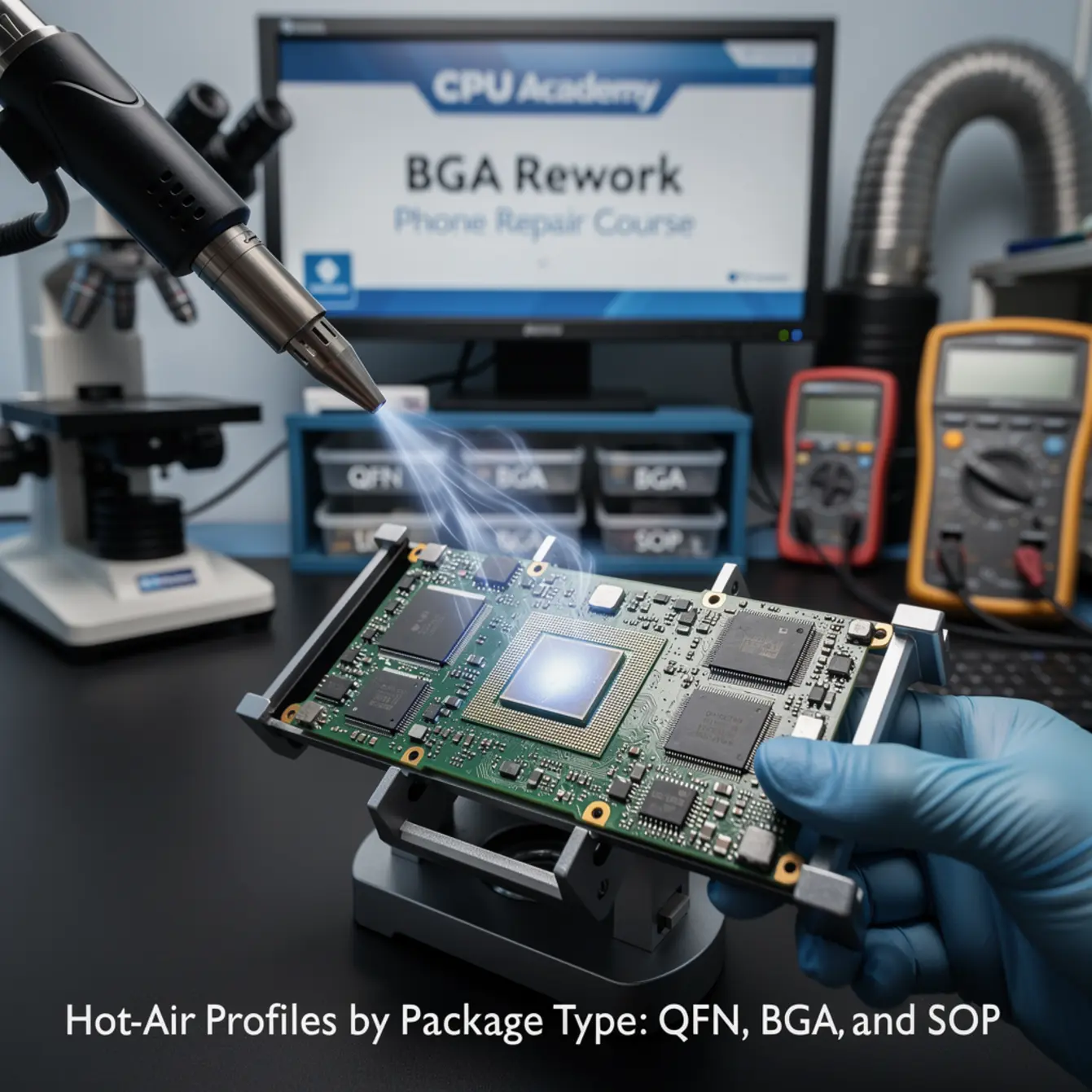
Core Workflow: Running the Right Profile
The four zones of a hot-air profile are the same regardless of package — but how long you stay in each zone, and at what temperature, shifts based on the chip in front of you.
The Four Zones
- Preheat / Ramp: Bring the board up slowly — aim for 1–3 °C per second. Too fast causes thermal shock. The whole board needs to come up together, not just the target chip.
- Soak Zone: Hold at roughly 150–180 °C for 60–90 seconds. This activates the flux, drives off volatiles, and equalises temperature across the package. Skipping this is the single most common beginner mistake.
- Peak Zone: Move into reflow territory. The solder needs to fully liquefy. See the table below for package-specific ranges.
- Cool-Down: Let the board cool naturally. Do not blast cold air on it — forced cooling before the solder solidifies causes cold joints every time.
Package-Specific Profile Reference
| Package | Soak Zone | Typical Peak Range | Airflow Priority | Primary Rework Risk |
|---|---|---|---|---|
| BGA | 150–180 °C, 60–90 sec | ~235–250 °C | Low — avoid displacing neighbours | Hidden cold joint; no visual confirmation of reflow |
| QFN | 150–180 °C, 60–90 sec | ~235–245 °C | Medium — even coverage over thermal pad | Thermal pad adhesion; flux voiding under centre pad |
| SOP/SOIC | 150–180 °C, 60–90 sec | ~230–245 °C | Controlled — pins are exposed | Bridging on fine-pitch; pad lift if ramp is too aggressive |
Source: Texas Instruments package soldering and reflow considerations. These are guideline ranges. Actual settings depend on board mass, layer count, and station calibration.
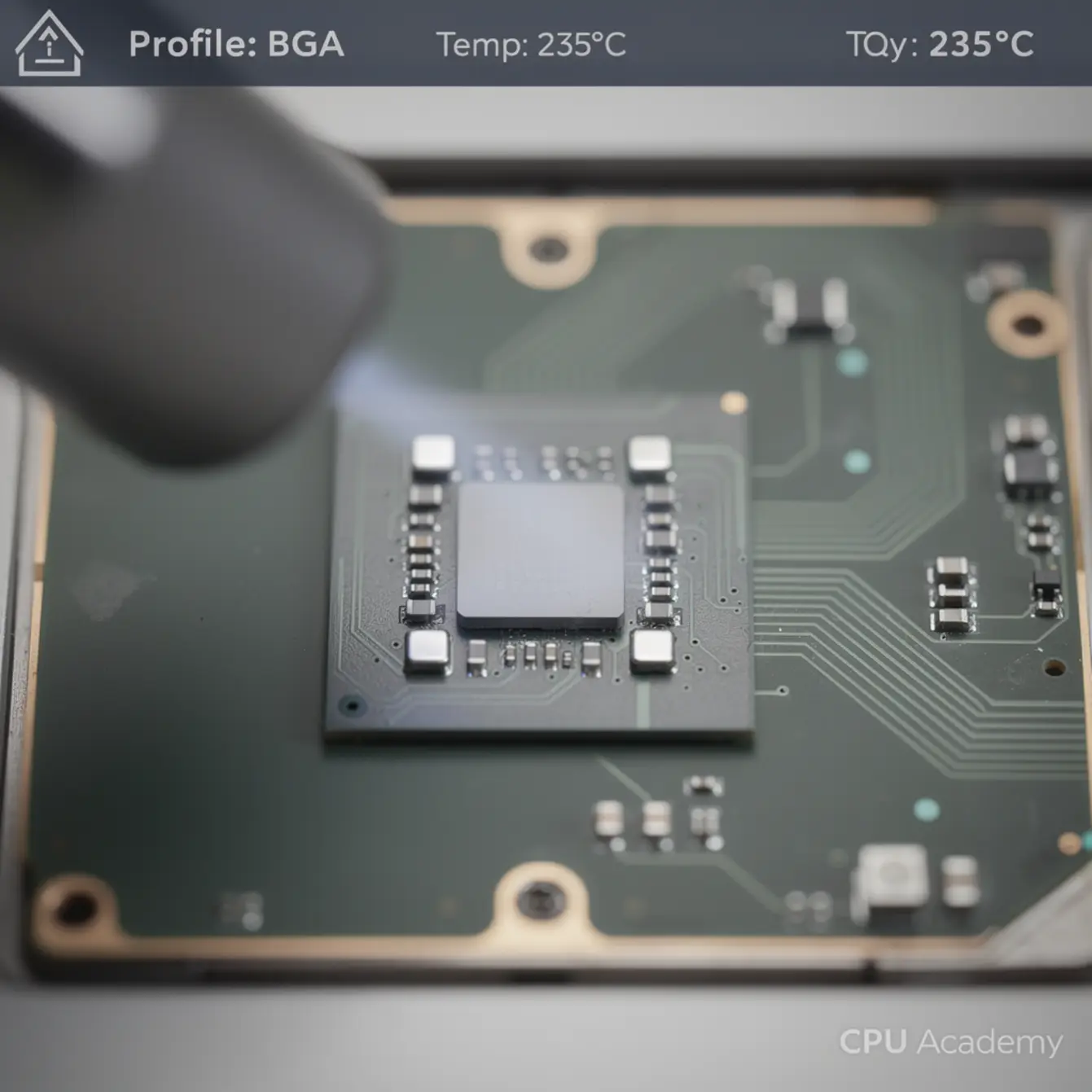
Heat Profile for BGA Specifically
BGA is the hardest because you’re flying blind. Apply flux under the package edge before heating. Watch for the chip to settle fractionally — that micro-drop is your visual cue that the balls have reflowed. If the chip lifts unevenly or rocks, something went wrong with the profile.
Keep airflow low enough that 0402 passives around the BGA don’t shift. A 3–5 mm nozzle standoff is a safe starting position; adjust based on your nozzle diameter and the chip footprint.
Flux Choice
No-clean gel flux is practical for most rework — it stays in place under the chip and cleans up with IPA. Avoid water-soluble flux on smartphone boards where full cleaning access is limited. For BGA reballing, use flux matched to your solder paste spec; mismatched flux activity levels cause solder balling during reflow.
Pad Protection
Mask any connectors, flex cable pads, or nearby chips with Kapton tape before firing up the station. Heat transfers fast on thin boards. A connector rated to 150 °C won’t survive sitting 4 mm from a peak-zone nozzle without protection.
Common Faults, Mistakes, and Recovery
Most rework failures trace back to one of a small set of causes. Knowing what each looks like — and what caused it — saves the board.
Fault Isolation Guide
| Fault | Most Affected Package | Root Cause | Recovery |
|---|---|---|---|
| Cold joint / no-reflow | BGA | Insufficient peak temp or soak time | Rework with corrected profile; verify with X-ray if available |
| Pad lift | SOP fine-pitch, QFN | Excessive temp or too-fast ramp | Pad repair with micro-wire; prevention is the only real fix |
| Tombstoning | QFN passive pads | Uneven heat across asymmetric pad | Reflow with nozzle centred more carefully; use preheat from below |
| Solder balling | BGA reballing | Flux residue + ramp too fast | Clean fully with IPA; reball with correct flux; slow the ramp |
| Bridging | SOP | Excess paste + uncontrolled heat | Wick excess solder; re-examine paste volume |
| Component displacement | All | Airflow too high during peak | Reduce flow; use nozzle that better concentrates heat |
Real Bench Scenario: The Boardshop QFN Miss
A technician reflowed a PMIC (power management IC) in a QFN package after a liquid intrusion repair. The phone powered on but ran hot and throttled within minutes. The fault: the centre thermal pad had partially lifted during removal because the ramp rate was too aggressive. The chip was making electrical contact but couldn’t dissipate heat properly.
The fix required a second removal, pad repair, fresh flux, and a slower profile with longer soak. The lesson — pad lift often doesn’t kill the phone immediately; it just makes it unreliable. That’s the kind of fault a customer returns for, and that turns a paid job into a warranty problem.
Rework QA
After every rework, clean flux residue with IPA and inspect under magnification before powering on. Look for lifted pads, displaced passives, and bridged pins on any SOP chips near the work area. Powering on a board with a flux-contaminated pad can cause shorts that weren’t there before you started.
How Schematic Thinking Speeds Diagnosis
Hot-air rework without schematic knowledge is guesswork. You apply heat to a chip, the phone works, you move on — but you don’t actually know what you fixed or why.
Schematics tell you what each IC is responsible for and which rails it sits on. That means before you touch a BGA, you already know whether the chip handles power delivery, audio, or baseband. You can probe test points around the package before and after rework to confirm the fault was solder-related rather than a dead chip. A dead chip won’t be fixed by reflowing it — and a reflow attempt on a chip with internal damage risks lifting pads for nothing.
There’s also a subtler benefit: some faults that look like solder faults are actually software faults. A corrupted baseband partition produces symptoms almost identical to a cold joint on the baseband IC. If you rework the chip first, you’ve wasted 20 minutes and put stress on the board. If you read the schematic and check the relevant test points first, you save the board and the time. The mobile phone software repair course at CPU Academy covers exactly that triage boundary — when to suspect software before you apply heat.
If you want to make hot-air rework reproducible rather than lucky, the Phone Schematic Diagram Course: Master iPhone & Board Repair at CPU Academy covers the diagnostic foundation you need. You’ll understand what the IC is supposed to do before you apply heat — and that changes everything about how you approach the bench.
This is the combination that turns micro soldering from a physical skill into a diagnostic discipline. And that’s the combination that makes it a higher-margin service: fewer comebacks, faster diagnosis, more confident quoting.
If you’re building toward offering board-level repairs as a service, the starting a mobile phone repair business course covers how to position and price that work so it’s actually profitable.
FAQ + Next Step
Frequently Asked Questions
- What hot-air temperature should I use to reflow a BGA chip?
- For SAC305 lead-free solder, a typical peak range is 235–250 °C at the board surface, reached after a slow ramp and a 60–90 second soak at 150–180 °C. Exact settings depend on your station’s calibration, the board’s layer count, and the chip’s thermal mass. Always verify surface temperature with a thermocouple probe rather than relying on station display alone.
- What is the difference between QFN and BGA rework?
- BGA joints are hidden under the chip, so you can’t confirm reflow visually. QFN has pads along the bottom edge plus a centre thermal pad — you can see the perimeter pads but not the central one. BGA requires lower airflow to protect nearby components; QFN needs even heat distribution to avoid voiding under the thermal pad. Both need the same four-zone profile approach, but the risk points are different.
- Is a BGA rework phone repair course worth it for someone already doing screen repairs?
- Yes — if you want to take on faults that screen-only shops turn away. Water damage, no-power boards, and boot-loop faults that originate at the IC level are all board-level work. Learning the skill opens a category of repair that commands higher margins and has less competition than screen replacements. The investment is in tools, training, and practice boards before you touch customer devices.
- What nozzle should I use for BGA rework?
- Use a nozzle sized close to the chip footprint — slightly smaller is preferable to slightly larger, so you’re not spilling heat onto adjacent components. Round nozzles work well for BGAs. Square nozzles suit QFN and SOP packages where you want to match the component outline. Always maintain a 3–5 mm standoff above the component surface as a starting point and adjust from there.
- Can I learn micro soldering without formal classes?
- You can build foundational skill through practice boards and online resources, but structured micro soldering classes reduce the number of boards you destroy learning by trial and error. More importantly, a course with schematic diagnosis built in teaches you to confirm faults before reworking — which is what separates reproducible results from lucky ones.
- How do I know if a BGA rework actually worked?
- Power on the device and test the specific function tied to that IC. Under magnification, look for the chip sitting flush without any rocking — uneven seating suggests incomplete reflow on one side. X-ray inspection is the definitive method, but most independent shops rely on functional testing and careful visual inspection of the package perimeter.
Your Next Step
The profiles in this guide give you a working framework. But the technicians who make board-level repair repeatable aren’t just running better profiles — they’re reading schematics before they fire up the station. They know which chip they’re working on, what it controls, and what a healthy board looks like on a multimeter before they apply heat.
Technicians who complete CPU Academy’s micro soldering course and schematic training take on board-level jobs they previously referred out — because they can diagnose before they rework, not just after. The BGA rework phone repair course skills you’ve built here are the physical foundation. The schematic layer is what makes them profitable.
Ready to move into full board-level diagnosis?
Open CPU Academy’s Phone Schematic Diagram Course: Master iPhone & Board Repair and move into the full advanced training path — where the profile work you’ve drilled here connects to the diagnostic logic that makes every rework count.