Quick Answer: Micro soldering training teaches technicians to apply controlled heat at board level without damaging plastic connectors, antenna traces, or RF shielding cans. The core skill is knowing which zones tolerate reflow and which do not — a distinction that separates a recovered board from a second fault. Training covers tools, technique, and thermal limits before live repair.
Picture this: the board powers up after rework, signal bars appear, then drop to zero thirty seconds later. The solder joint looks fine. The damage happened somewhere else, in a zone you heated without realizing how sensitive it was. That moment is frustrating, but more importantly, it is avoidable.
If you are already doing basic phone repair and want to move into board-level work, understanding heat-sensitive zones is the single most protective habit you can build first. It is not the glamorous part of the job. But it is what keeps you from creating two problems while fixing one.
This guide covers the two zones that get damaged most often — plastics and RF areas — the tools that guard them, the workflow that keeps repairs clean, and the faults that show up when things go sideways. Everything here reflects real bench practice. There is no theory invented for the page.
Worth noting up front: The workflow below lines up with structured board-level repair content, including the schematic-first diagnostic method taught inside CPU Academy’s Phone Schematic Diagram Course: Master iPhone & Board Repair. Reading the schematic before applying heat is not optional at this level. It is the first step, full stop.
What This Skill Is and When It Matters
Heat management during board-level repair means directing thermal energy precisely enough to reflow a target joint without raising the temperature of everything beside it to a damaging level. That sounds simple. On an actual smartphone PCB, with components packed within a couple millimeters of each other, it takes real discipline to pull off consistently.
Two categories of components fail from mis-applied heat more than anything else: plastic structures and RF zones. Both sit right next to the high-value BGA and PMIC pads you are actually trying to rework. That proximity is the whole problem.
Plastic components at risk
FPC connectors — the white or black latched sockets for display cables, cameras, and battery leads — are made from thermoplastic housings that deform well below typical reflow temperatures. The retainer clips are especially fragile. They are thin, they are close to everything, and they do not give you any warning before they melt.
SIM tray anchor points are moulded into the board at positions that often sit directly beside logic circuitry. When a clip melts, the cable no longer seats correctly. The result is an intermittent fault that shows up after reassembly and is nearly impossible to trace without cracking the phone open a second time.
RF zones at risk
RF shielding cans cover the sections of the board that handle antenna signals, cellular modem data, and Wi-Fi. They are soldered in place during original assembly. Secondary reflow from your repair can cause the can’s own solder to flow, shift the can slightly, and break the seal or lift an antenna pad underneath.
Antenna feed pads and coaxial cable termination points are similarly vulnerable. Flux residue left under an RF can after rework is a classic post-repair fault pattern. It traps moisture, and the board develops intermittent signal drops days or even weeks after the repair seemed successful.
You are often trying to reflow something important within 2 to 5 mm of something that must not move at all. That gap demands precision, not speed. Bravado with the hot-air station is how boards get ruined.
Bench Setup, Tools, and Safety for Micro Soldering Training
The right tools do not guarantee a clean repair, but the wrong tools make board damage almost certain. Here is what a functional heat-sensitive rework station actually looks like, and why each item earns its place on the bench.
Microscope setup
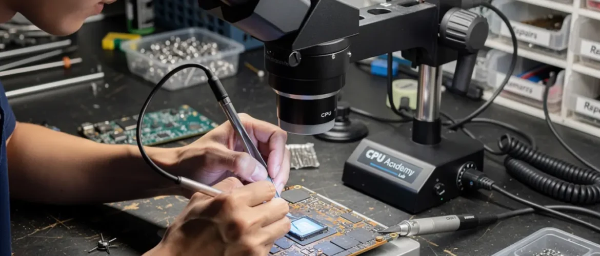
Magnification between 10x and 45x is the minimum for this class of work. Without it, you cannot place tape accurately, you cannot see whether flux has crept under an RF can, and you cannot catch the visual reflow cue that tells you to pull the heat back. Microscope fatigue is real too — staring through the eyepieces for long sessions without a proper arm position leads to rushed decisions and sloppy tape placement, both of which cost you boards. A trinocular arm is useful if you record repairs for review. The microscope is not optional. It is how you confirm that every other tool is positioned correctly.
Hot-air rework station
A station with independent airflow and temperature control, such as the Hakko FR-810 or FR-872, lets you set airflow first and temperature second. That order matters because high airflow at the wrong angle physically moves small components off their pads before the solder even flows. Nozzle selection controls the radius of heat. A concentrator nozzle limits spread to roughly the target component footprint and gives you far more control near sensitive zones. See Hakko’s hot-air rework safety and handling guidance for nozzle maintenance detail worth reading before you swap tips.
Heat profile and flux choice
Low-melt solder, specifically bismuth-tin alloys, reduces the peak temperature needed to achieve flow. Near plastic zones, that matters a lot. Lower peak temperature means shorter dwell time, which means less heat conducted into adjacent structures. Flux choice affects how cleanly the joint flows and how much residue you are left managing afterward.
Flux control is a bigger deal than most beginners expect. Using too much flux near an RF can means you are cleaning a problem you created yourself. Use flux appropriate to the alloy, apply it deliberately, and remove residue thoroughly before replacing any RF shield can.
Pad protection: Kapton tape
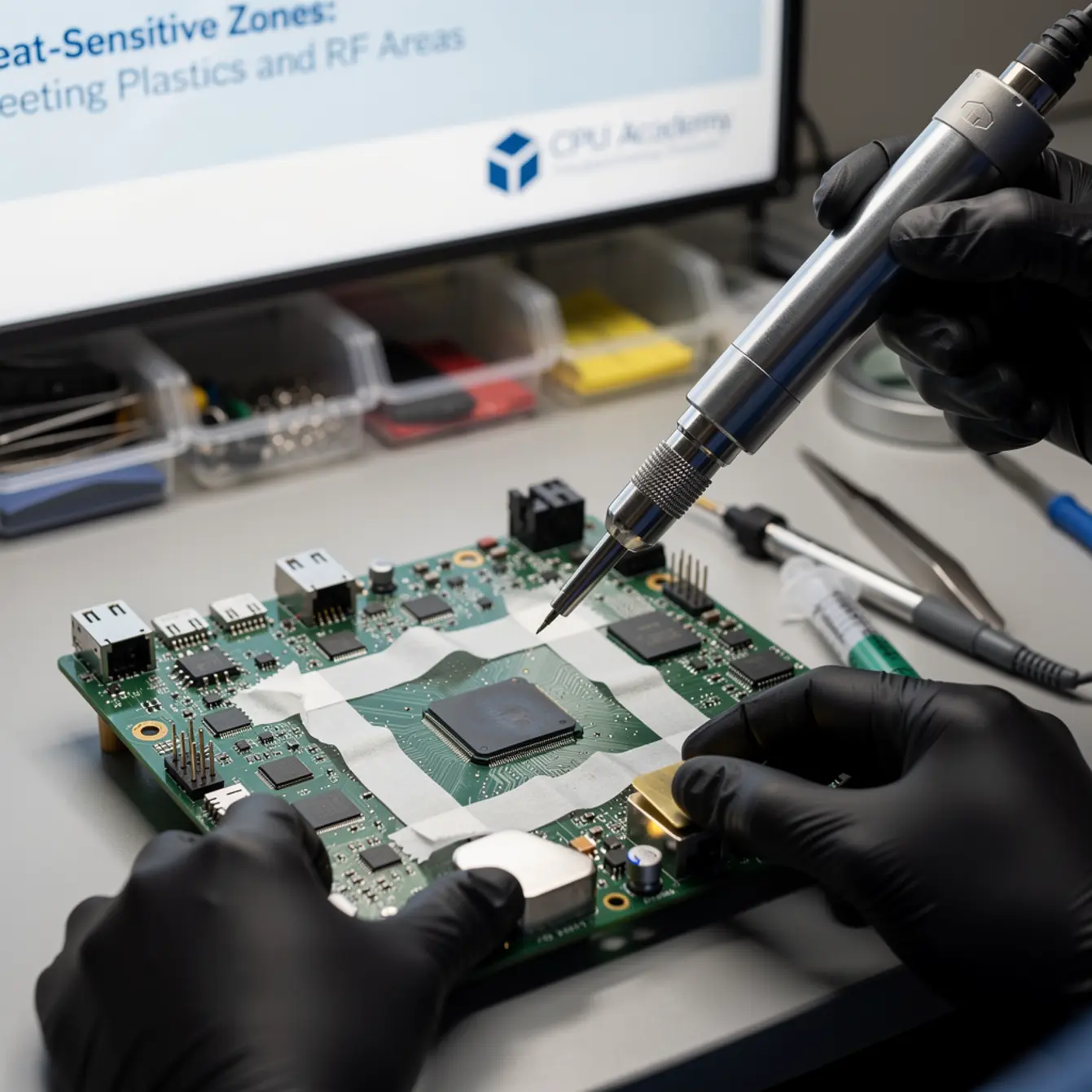
Thermally stable polyimide tape, the stuff people call Kapton, is the primary physical shield for plastic components. Placed correctly, it intercepts the hot-air stream before it reaches an FPC latch. Placement must be checked under magnification. Tape that overlaps a target pad causes an incomplete reflow. Tape placed 1 mm too far from a latch offers no real protection. One pass under the microscope before you pick up the hot-air station saves you a lot of grief later.
| Tool | Role in heat-sensitive rework | Critical detail |
|---|---|---|
| Hot-air rework station | Directed reflow with controllable radius | Set airflow before temperature; choose concentrator nozzle |
| Kapton/polyimide tape | Shields plastic connectors from direct airstream | Place under magnification; do not overlap target pad |
| Low-melt solder (Bi-Sn) | Reduces peak temperature needed to achieve flow | Useful near FPC zones; clean flux residue fully |
| Microscope (10–45×) | Confirms tape placement, reflow cue, and post-repair cleanliness | Not optional at board level |
| Brass or silicone tip shields | Protects FPC latches from direct hot-air contact | Useful when tape alone cannot cover the geometry |
| No-clean flux pen or paste flux | Promotes clean joint flow; reduces cold-joint risk | Remove residue under RF cans even with no-clean types |
Core Workflow for Reflowing Near Plastic and RF Zones
A repeatable sequence is what keeps repairs consistent across boards and across different days on the bench. Skipping steps, especially the schematic check and the tape stage, is where boards get damaged. Not sometimes. Reliably.
- Schematic check. Identify which nets carry antenna signals and which FPC connectors sit on adjacent power rails. This tells you exactly which zones need protection before you touch the board. CPU Academy’s board-level phone repair course integrates this check as a standard pre-heat step, not an afterthought.
- Visual inspection under magnification. Look for existing damage, lifted pads, or prior rework that changes how heat will conduct through the board. An already-damaged pad changes your approach entirely. You need to know that before you apply any heat.
- Pre-tape all plastic components within thermal reach. Work outward from the target pad. Every FPC latch, retainer clip, or moulded housing within 5 mm of the target gets covered. Then inspect placement under the microscope before moving forward.
- Select the correct nozzle; set airflow before temperature. A smaller nozzle concentrates heat but requires slower movement. A wider nozzle covers the target faster but risks heating adjacent zones. Match the nozzle to the target footprint, not to what feels convenient.
- Approach angle: never direct the airstream toward an FPC latch. Come in at an angle that pushes hot air away from plastic housings. If the geometry forces you toward a latch, add a silicone tip shield or brass block as a secondary deflector.
- Monitor visual reflow cues; do not time-guess. Watch for solder to transition from dull to liquid-bright at the joint. Pull heat the moment you see that shift. Counting seconds instead of watching the joint is how over-heating happens.
- Cool-down before removing tape; inspect before reassembly. Let the board reach ambient temperature with tape in place. Remove tape slowly — adhesive left on a pad causes assembly faults. Inspect every protected zone under magnification before you close the device.
Rework QA: what to check before the board leaves the bench
After cooling, run through this list: joint sheen is consistent with no cold joints adjacent to the target, all FPC latches open and close freely, no tape residue is sitting on any pads, flux is fully removed from under any RF can that was disturbed, and antenna coaxial connectors re-seat with a positive click. That last one is easy to rush. Do not rush it.
Common Faults, Mistakes, and Recovery
Most heat-related board damage follows predictable patterns. Each fault below has a cause, a visible sign, and a clear prevention rule. Recognizing these before they happen to you is the fastest way to build heat discipline that actually sticks.
Fault isolation: lifted antenna pads
Cause: Too much dwell time or too-high airflow pressure pulling the pad from the board surface during reflow.
Observable sign: The pad moves with the solder, leaving a bare area on the PCB substrate.
Prevention rule: Watch the visual reflow cue and pull heat the moment solder transitions. Never use airflow pressure to push solder into position.
Melted FPC latch
Cause: Kapton tape not placed, or placed inaccurately, leaving the latch directly exposed to the hot-air stream.
Observable sign: The latch housing is warped or fused open. The cable no longer seats securely.
Prevention rule: Place tape under magnification before every rework session. There is no shortcut here, and heat discipline matters more than saving thirty seconds on prep.
Post-repair signal drop from flux under RF can
Cause: Flux applied near an RF shield can migrated under it during reflow and was not cleaned before the can was replaced.
Observable sign: Cellular or Wi-Fi signal is intermittent, typically worse in humid conditions or after the device warms up from use.
Prevention rule: Remove the RF can deliberately, clean the area with isopropyl alcohol, and inspect under magnification before replacement. This is one of the most common post-repair fault patterns in board-level work, and it is entirely avoidable.
Delaminated flex cables
Cause: The copper-clad polyimide layers in flex cables begin to delaminate at elevated temperatures. A typical threshold for polyimide is around 260°C, though treat that as a conservative reference point rather than a certified spec for any specific product.
Observable sign: The flex cable bubbles, discolors, or goes rigid near the rework area.
Prevention rule: Keep the hot-air nozzle directed at the target pad, not the flex routing. Low-melt solder helps here by reducing the peak temperature you need to reach.
Case example — intermittent signal after PMIC rework:
A technician reworks a PMIC on a smartphone board without removing the adjacent RF shield can. After reassembly, the device shows full bars, then drops to no service after about two minutes of use. The board goes back under the microscope. Flux residue is visible along the seam of the RF can directly above the rework zone.
The can comes off, the area gets cleaned, and the can is resoldered. Signal fault does not return. Total additional time: roughly 25 minutes. The fault was entirely preventable with one extra cleaning step before the initial reassembly. That is the real cost of skipping steps.
How Schematic Thinking Speeds Diagnosis
Knowing where every antenna net and FPC power rail sits on the board before you apply heat is what separates a controlled repair from an educated guess. The schematic is your map. Without it, you are navigating by feel in a space where mistakes are expensive.
When you identify that a particular net carries the main antenna signal, you know exactly which pads and traces to keep tape-protected. When you can see which FPC connector feeds the display backlight, you know that heating the adjacent PMIC zone puts that connector at risk, even if it looks physically distant on the board surface.
This is why reading a schematic is not an advanced add-on to board-level repair. It is the first diagnostic step. Without it, you are making proximity guesses rather than decisions grounded in actual circuit knowledge.
Fault isolation using the schematic
When a post-repair fault appears, say a cellular signal drop, the schematic lets you trace the antenna net back to every component on that path. You do not have to inspect the whole board. You inspect the two or three components on that specific net, in order of thermal exposure during your rework. That is a focused, efficient process.
For anyone working through a board level phone repair course, this is the practical payoff of schematic-based diagnosis. It converts a vague signal problem into a short, ordered checklist of specific components to check. The difference in time spent troubleshooting is significant.
The Phone Schematic Diagram Course: Master iPhone & Board Repair at CPU Academy walks through reading iPhone and Android schematics at exactly the level this kind of board-level diagnosis requires. That means identifying RF nets, FPC rails, and power domains before heat ever touches the board. If schematic reading is currently your gap, that course closes it directly.
For broader context once the hardware habits are in place, the Mobile Phone Software Repair Course and the guidance inside Starting a Mobile Phone Repair Business round out the full picture.
FAQ and Next Step
What parts of a phone PCB are most heat-sensitive?
FPC connectors for the display, camera, and battery leads, along with retainer clips, SIM anchor points, RF shielding cans, antenna feed pads, and coaxial cable termination points. All of these sit within a few millimeters of the BGA and PMIC pads most commonly reworked. That proximity is exactly why they get damaged so often by mis-applied heat.
Do I need to understand schematics to do micro soldering?
Yes, at board level. You do not need to design circuits, but you need to read enough of a schematic to identify which nets carry antenna signals and which FPC connectors share a power rail with your target component. Without that, you are protecting zones by guesswork rather than circuit knowledge. A structured micro soldering course that includes schematic reading closes this gap in a way that unstructured practice simply cannot.
What is the correct sequence for reworking near RF shielding cans?
Check the schematic to confirm which nets the can covers, then remove the can deliberately rather than heating through it. Clean all flux from the area before any reflow. Complete your target rework, then clean again. Replace the can with fresh flux and inspect the seal under magnification before reassembly. Skipping the cleaning steps is the most common cause of post-repair signal faults in this zone.
Is micro soldering training worth it for an intermediate repair technician?
If you are already doing screen and battery swaps and want to move into board-level faults like no-power boards, logic failures, and signal issues, then structured micro soldering classes add the systematic workflow that self-taught practice rarely builds on its own. The main gaps closed are schematic-based zone identification, correct tool sequence, and post-repair inspection discipline. Those three habits are what prevent board-level repairs from producing second faults.
What is the next practical step after reading this guide?
The most direct next step is learning to read the schematics for the boards you work on. That skill connects to every section of this guide — zone identification, fault isolation, and post-repair QA all depend on knowing what the schematic shows before the hot-air station comes out.
Ready to move from this guide into the full skill path?
This topic gets much easier when you see the full sequence laid out in a structured format. If you are serious about board-level work, micro soldering training built around real schematic reading is the clearest path forward. Open CPU Academy’s Phone Schematic Diagram Course: Master iPhone & Board Repair and move into the full advanced training path, starting with the schematic skills that make every heat-sensitive repair safer and more repeatable.