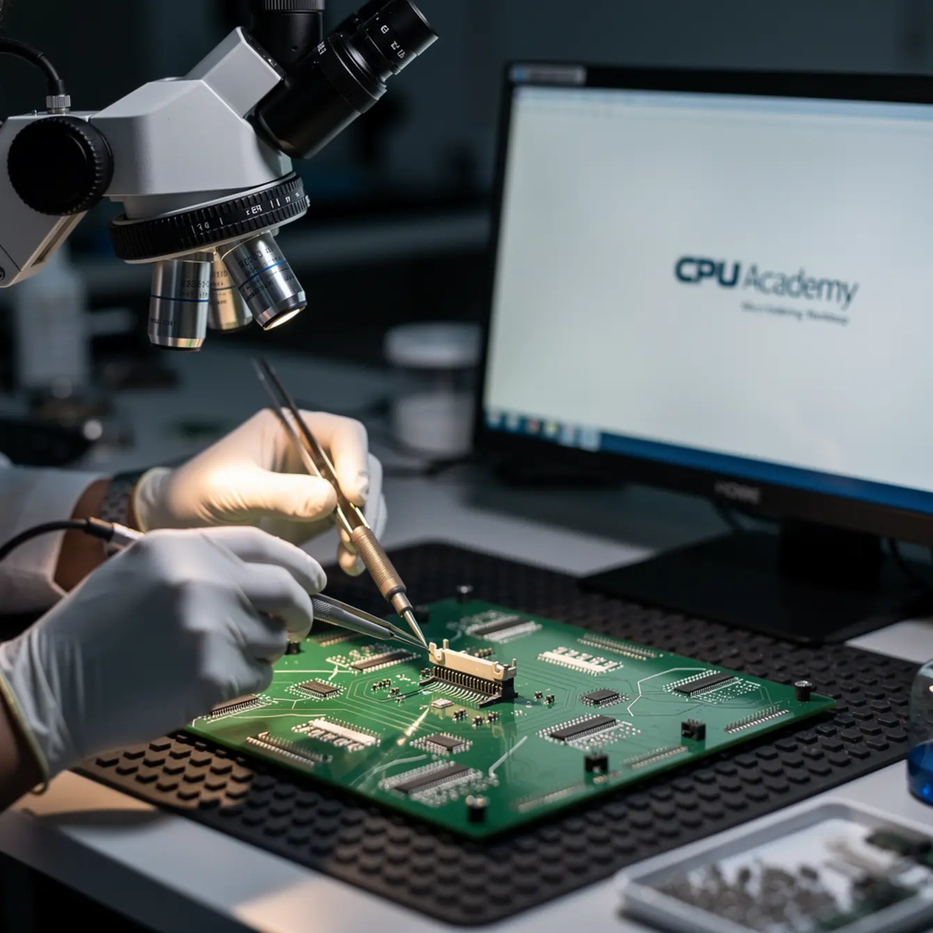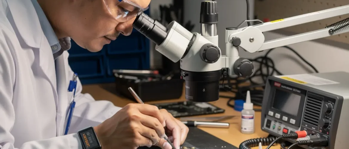
Quick answer: Micro soldering training teaches technicians to seat, anchor, and reflow connectors at the board level without bridging pads or lifting traces. The three highest-failure points are pad-to-footprint misalignment, inadequate mechanical anchoring, and unintentional solder bridges — each correctable with the right toolset, flux discipline, and schematic verification before any heat is applied.
You pick up the board. The connector is off by half a millimetre. Under the microscope it looks like an impossible puzzle — tiny pads, tight pitch, no obvious way in. That moment is exactly where most beginners freeze and most intermediates make a costly mistake.
Here is the good news: connector footprint work becomes manageable the moment you break it into three clean problems. Alignment, anchoring, and solder bridges. This guide walks through all three in plain English, with real bench workflow and zero fluff.
This article is written for US technicians who already handle basic screen and battery swaps and now want the board-level skills that come with higher-margin repairs. Solid micro soldering training starts here, and so does understanding why these three problems matter more than any single tool you could buy.
What this skill is and when it matters
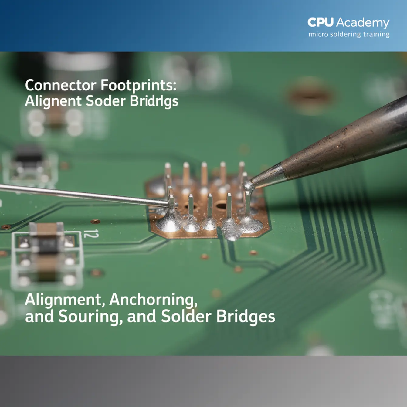
Every connector on a mobile logic board sits inside a footprint — a precise copper pad pattern, courtyard boundary, and silkscreen outline that tells solder exactly where to flow and tells the assembly exactly where to stop. When a connector is damaged, corroded, or torn from the board, you are not just replacing a part. You are rebuilding a precise mechanical and electrical interface at sub-millimetre scale.
Three things will end a repair before it starts if you skip them: seating the connector straight on its pads, reflowing the mechanical anchor tabs alongside the signal pads, and clearing any unintended solder bridges between adjacent pads. Miss any one and the repair either fails electrically or breaks again under normal use — sometimes within days.
This matters most on fine-pitch board-to-board connectors, ZIF and FPC sockets, and battery connectors, all of which are common in modern smartphones. If you are serious about a board-level phone repair course, connector footprint work will show up in your first real case. It is not advanced in the scary sense. It is just precise — and precision is learnable.
Bench setup, tools, and safety for micro soldering training
Microscope setup
A stereo microscope in the 7x to 45x zoom range is non-negotiable for this work. Set your working distance so both hands move freely under the objective without you craning your neck forward. That posture matters more than people admit — hunch toward the eyepieces and your hands lose steadiness fast. Start every session at low zoom for general orientation, then step up to 20x or higher for pad inspection and bridge detection.
Heat profile and station choice
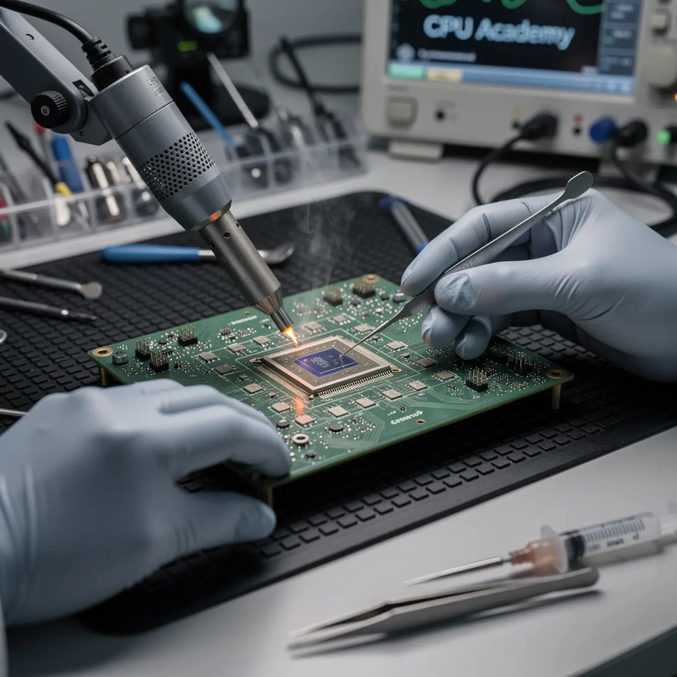
Use a temperature-controlled iron with a fine conical or knife tip, kept at or below 350°C for most mobile connectors. A hot-air rework station with an adjustable nozzle handles full connector removal. Keep air volume low near connectors to avoid disturbing adjacent components. The 200 to 380°C range covers most scenarios, but always check the connector’s datasheet for tighter limits before you dial anything in.
Flux choice
No-clean gel flux is the standard for connector work. It holds the connector in place during pre-positioning, promotes even solder flow, and reduces bridge formation on fine-pitch pads. Liquid flux works well for wicking existing bridges. Either way, use a measured amount. Too much flux traps under the connector body and hides bridges during post-clean inspection, which is the last thing you want after you have already spent twenty minutes on alignment.
Pad protection
Before applying any heat, mask adjacent flex cables and plastic housing with Kapton tape. Mobile boards pack a lot into a very small space, and hot-air work near an unmasked flex will melt it. This step takes thirty seconds and saves you from a much worse repair.
Bench tool checklist — connector footprint work
| Tool | Why it matters |
|---|---|
| Stereo microscope (7x–45x) | Reveals pad offset, bridge formation, and cold joints invisible to the naked eye |
| Hot-air rework station (200–380°C) | Uniform reflow for full connector removal or seating |
| Temperature-controlled iron + fine tip | Pin-by-pin work, bridge clearing, anchor pad reflow |
| No-clean flux (gel or liquid) | Pre-positioning tack, solder flow control, bridge prevention |
| Fine solder wick (pre-fluxed) | Bridge removal without adding more solder |
| IPA 99%+ and lint-free swabs | Post-rework cleaning to reveal hidden bridges |
| Brass wire tip cleaner | Tip maintenance without thermal shock |
| Anti-static mat and wrist strap | ESD protection — ZIF connectors have direct paths to sensitive ICs |
| Fine-point reverse-action tweezers | Connector placement and hold during reflow |
| Kapton tape | Heat masking for adjacent flex cables and plastic parts |
| Digital multimeter (continuity mode) | Post-repair verification of signal and anchor pad connections |
| Phone schematic diagram | Pin-1 orientation, pad assignment, and bridge diagnosis |
Safety notes you should not skip
ESD is a real risk on this work. Fine-pitch connectors route directly to application processors and power management ICs. One static discharge through an ungrounded technician can kill a chip you never touched with the iron. Always use the mat and wrist strap, every single session.
No-clean flux still produces irritant vapour at rework temperatures. Run a fume extractor or ensure solid lateral airflow at the bench. IPA cleaning should only happen on a powered-off board, and give it full dry time before powering back on. Rushing that step has burned more than a few people.
Core workflow — the connector footprint fix path
Good connector rework follows a repeatable sequence. Skipping steps is where most mistakes happen, and the steps that get skipped most often are always at the beginning and the end.
- Read the schematic first. Identify pin 1, the anchor pad locations, and any pads that share a ground pour. Doing this before heat goes anywhere is what separates trained technicians from people who get lucky. CPU Academy’s board-level curriculum pairs schematic reading with physical rework so technicians verify pad assignments before picking up the iron — which eliminates the single most preventable cause of connector damage.
- Inspect the pads under magnification. Check for lifted pads, oxidation, excess old solder, or damage from a previous repair attempt. Deal with all of this before placing the new connector. A lifted pad that looks minor at bare eye is obvious at 20x, and a pad can lift even further if heat stays on it too long during rework, so catch it now.
- Clean and re-tin the pads. Use solder wick to level the pad surface, then apply a thin fresh tin layer. This gives the new connector an even solder base and reduces the chance of bridges forming during reflow.
- Dry-fit the connector without solder. Place the connector under the microscope and verify alignment by eye at 10x or higher before any flux or heat is involved. Check that all rows sit over their correct pads and the body lies flat with no rocking at any corner.
- Apply gel flux and reflow. Tack one corner pad first to lock position, then reflow the remaining signal pads with the iron or hot air depending on connector pitch and size. Work methodically down each row, not jumping around.
- Reflow the anchor pads. These are the mechanical strain-relief tabs. They carry the physical stress of cable mating and unmating. Skipping them is a common error — the connector passes an electrical test but fails in normal use within days.
- Clean and re-inspect. Apply IPA, let it dissolve the flux residue, then examine the entire footprint under the microscope before testing anything. Flux residue hides bridges. The job is not done until the pads are visible and confirmed clear.
- Continuity test. Use your multimeter in continuity mode against the schematic to confirm each signal pad connection and verify no shorts between adjacent pins. This is your final check before the board sees power.
Common faults, mistakes, and recovery
Fault isolation — the three categories
Alignment faults usually show up as partial signal loss or intermittent function. The most common is a 180-degree rotation on a connector housing that looks symmetrical from above — always confirm pin 1 from the schematic before you start anything. A pad-row offset, where the connector is shifted slightly along the X or Y axis, will bridge wrong pads while leaving others open. Your eye will not catch this reliably. Magnification will.
Anchoring faults show up later, not immediately. The phone works fine for two days, then the connector lifts under cable strain. Signal pads were never designed to carry mechanical shear load. The anchor tabs exist exactly to take that load off the signal pads. Reflow them every single time, with full solder volume, confirmed under the microscope before you close the case.
Solder bridges are the most immediately diagnosable fault — you see a short on the multimeter right away. They form when solder volume is too high, tip geometry is wrong for the pad pitch, flux quantity is off, or the technician moves too fast across the row. Recovery is straightforward: apply fresh gel flux to the bridge, then wick with fine pre-fluxed braid. The flux lowers surface tension so the wick pulls the bridge cleanly without disturbing adjacent pads. Never drag a dry wick across fine-pitch pads. It drags solder into the neighbouring pads and turns one bridge into three.
Rework QA — the post-repair checklist
- All pads visible under microscope after IPA clean? ✓
- No solder bridges between adjacent pads? ✓
- Anchor tabs reflowed with full, shiny fillet? ✓
- Continuity confirmed on all signal pins vs. schematic? ✓
- Connector body flat — no rocking at any corner? ✓
- Adjacent flex and housing undamaged? ✓
- Board powered off and fully dry before functional test? ✓
Case example: battery connector — bridge on the B+ pad
A technician replaces a torn battery connector on an iPhone logic board. After reflow, the phone shows no charge response. Continuity test flags a short between the B+ pad and an adjacent ground pad — a textbook solder bridge sitting hidden under flux residue.
Recovery path: IPA clean first to expose the bridge visually. Apply fresh gel flux directly to the bridged area. Press fine solder wick flat against both pads and touch the iron lightly — three seconds maximum. Lift the wick and iron together, not sequentially. Re-inspect under 20x. The bridge is gone. A second continuity check clears the short. The phone charges normally after functional test.
Root cause: Excess solder volume on the B+ pad during re-tinning, compounded by no flux being applied before the first wick attempt. The fix took four minutes once the cause was identified. Without a schematic to confirm which pad carried the B+ line, diagnosing that short would have taken much longer and could have led to unnecessary heat cycles on a board that had already been stressed.
How schematic thinking speeds diagnosis
A schematic is not optional for connector work. It is the tool that makes every other tool more effective. Without it, you are guessing which pad carries which signal, which pins are ground, and which anchor tabs are electrically floating. With it, you can identify a likely bridge before you even probe the board.
Consider a practical example. A ZIF connector on a phone’s display assembly has 40 pins at 0.4 mm pitch. Two adjacent pins might both appear to be ground when you look at the board. But the schematic shows one is a display enable line and the other is a true ground. A bridge between them kills the display without triggering a dead-short reading on your meter. You would never find it by probing randomly. You find it in under a minute by checking the schematic and probing the exact pair.
For technicians moving from basic screen swaps into connector rework, CPU Academy’s Phone Schematic Diagram Course: Master iPhone & Board Repair closes the gap between reading a schematic and acting on it safely at the bench. The course covers schematic navigation alongside physical repair context, which is exactly the combination that makes connector-level diagnosis feel less like guesswork and more like engineering.
Reading a schematic also gives you the courtyard boundaries for each footprint. That tells you exactly how far your hot-air nozzle can travel before it risks disturbing a neighbouring component. You are not estimating safe clearance based on feel. The document gives it to you directly, and that specificity is what separates fast, confident rework from slow, anxious rework.
If you hit a case where the board fault seems hardware but the phone’s behaviour suggests something else — camera failing after a connector repair, for instance — a quick look at the mobile phone software repair course at CPU Academy helps you rule out software stack issues before you go back to the board with more heat.
The outbound reference that informed the pad geometry and courtyard conventions in this article is worth bookmarking: Samtec PCB footprint design resources covers land-pattern definitions in more technical depth than most repair-focused guides do.
FAQ + next step
What is a solder bridge and how do you fix it?
A solder bridge is an unintended connection between two adjacent pads caused by excess solder, insufficient flux, or the wrong tip geometry for the pad pitch. Fix it by applying fresh gel flux to the bridged area and pressing fine pre-fluxed solder wick flat against the bridge with a clean iron tip. The flux lowers surface tension so the wick absorbs the excess cleanly without pulling solder into neighbouring pads. Re-inspect under magnification after cleaning with IPA, and confirm continuity is clear before calling it done.
Do I need a microscope for connector footprint work?
Yes, without question. Modern smartphone connectors use pad pitches of 0.4 to 0.5 mm, which is smaller than the diameter of a standard mechanical pencil lead. Alignment errors and bridges at this scale are invisible to the naked eye. A stereo microscope in the 7x to 45x range is the minimum for safe, accurate connector work. There is no shortcut around this one.
Can I learn connector rework through a micro soldering course online?
Yes. Online micro soldering classes can teach the theory, workflow, and schematic reading that underpin safe bench practice. The physical skills — tip control, heat management, flux application — still need real hands-on time at an actual bench. The best online micro soldering course options combine schematic instruction with clear rework walkthroughs so you arrive at the bench with a clear mental model, not just vague familiarity with the vocabulary.
Why do anchor pads matter if the connector passes an electrical test?
Electrical continuity and mechanical strength are two completely different things. A connector can pass every signal test immediately after rework and still fail within days if the anchor tabs are not properly reflowed. The tabs carry the physical stress of cable mating and unmating. Without them, the signal pads carry shear load they were never designed to handle, and they eventually lift from the board — sometimes taking traces with them.
Is board-level connector repair worth learning as a business skill?
Most independent repair shops send board-level work to specialists or decline it entirely. Technicians who can handle connector footprint repair, BGA rework phone repair course material, and chip-level diagnosis take on jobs that shops without those skills turn away. That translates directly to higher-margin work and a reputation that attracts more referrals. If the business angle interests you, CPU Academy covers the path in detail through its starting a mobile phone repair business course.
What is the next step after this guide?
The clearest next step is building your schematic reading skills alongside your physical rework habits. Connector work without schematic knowledge is slow and error-prone. With it, diagnosis is faster, bridge identification is precise, and pad assignments are confirmed before heat ever touches the board. That combination is where real phone chip level repair training starts to pay off.
Ready to go deeper with real micro soldering training?
Connector footprint work rewards technicians who understand what they are looking at before the iron goes on. The skill that makes the biggest difference at this stage is learning to read phone schematics at the same level you work at the bench — not as a separate academic exercise, but as a live diagnostic tool.
If you are serious about board-level work, don’t stop at the blog version. Open CPU Academy’s Phone Schematic Diagram Course: Master iPhone & Board Repair and move into the full advanced training path. It is built for technicians who are chasing higher-margin repairs and want schematic-guided bench habits that hold up under real case pressure — which is exactly where connector footprint mastery leads.