
Blog
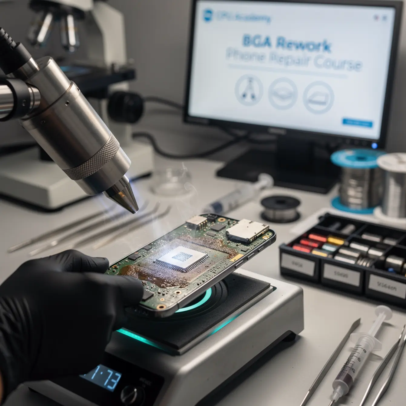
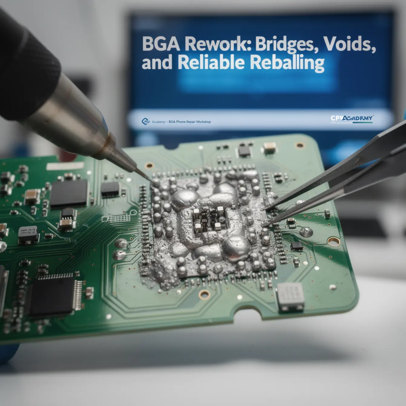
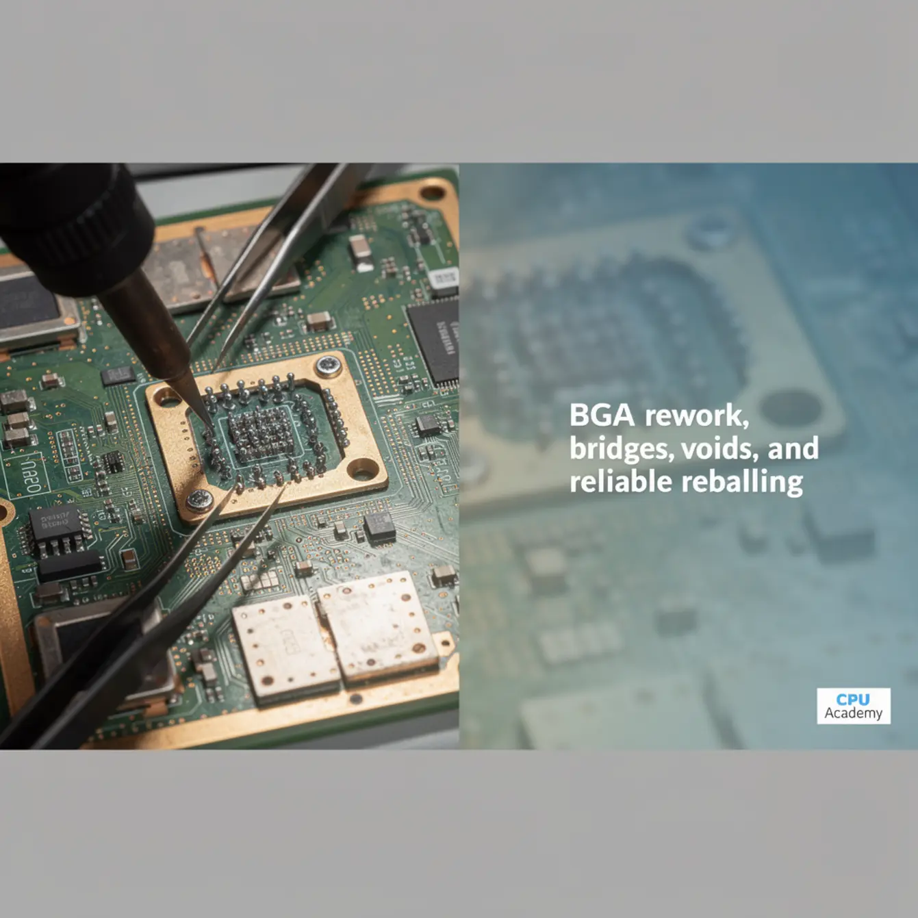
BGA Rework: Bridges, Voids, and Reliable Reballing
BGA Rework: Bridges, Voids, and Reliable Reballing
A BGA rework phone repair course teaches technicians to remove, clean, reball, and reflow ball-grid-array chips on smartphone motherboards using hot-air stations, infrared preheaters, and flux. It covers solder bridges, voids, and alignment faults — the three failure modes that cause most board-level rejections after chip replacement.
- Bridges — unintended solder shorts between adjacent balls
- Voids — gas pockets trapped inside a joint during reflow
- Misalignment — chip shifted off pad during placement or reflow
Each fault has a different cause, a different detection method, and a different fix path.
By the CPU Academy Content Team | Board-level repair specialists
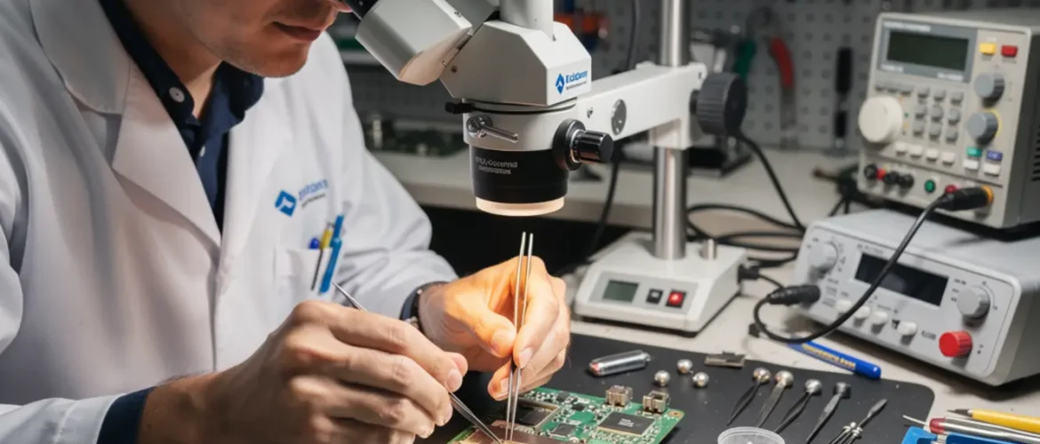
The first time you look at a phone motherboard under a microscope, the repair looks impossible. Chips the size of a fingernail, solder balls you can barely see, and zero margin for a shaky hand. Then someone shows you the workflow — and everything changes.
This guide is for technicians who already handle screen and battery swaps and want to move into board-level work. Higher skill, higher margin, and a completely different tier of repair jobs. Before you commit to a BGA rework phone repair course or put a hot-air gun anywhere near a live board, you need the minimum working knowledge covered here.
Reading a board schematic is foundational before you touch any chip. The Phone Schematic Diagram Course: Master iPhone & Board Repair at CPU Academy maps the pad locations and circuit paths you will need to identify before you start rework — it’s worth opening that before you go further.
What BGA Rework Means — and When It Matters
BGA rework on a phone board means using controlled heat to lift a chip, clean the pads, apply new solder balls to the chip’s underside, and reflow it back to spec — without damaging surrounding components.
BGA stands for Ball Grid Array. Instead of pins on the edges, the chip connects to the board through a grid of tiny solder balls hidden underneath it. You cannot see them during assembly. That’s both the advantage — incredible density in a small package — and the challenge when something goes wrong.
Smartphones lean heavily on BGA packaging for components like the CPU, NAND flash, PMIC (power management IC), and Wi-Fi modules. The ball pitch on these chips is tight — fractions of a millimeter — which is why smartphone board-level work requires dedicated tooling and a steady process.
Reflow vs. Reball — Two Different Interventions
Reflow means applying heat to re-melt the existing solder balls and re-seat the chip. You use this when balls have gone cold, cracked, or partially voided but the chip and pads are otherwise undamaged.
Reballing means fully removing the old balls, cleaning the chip’s underside, and applying a fresh set of solder balls using a stencil matched to the chip’s footprint. You use this after a full lift, after corrosion damage, or when a reflow alone cannot produce a clean joint.
Common triggers for BGA rework include water-damage corrosion on pads, failed software update bricks tied to NAND faults, factory voids that survived initial assembly but failed under thermal stress, and previous repair attempts that left bridges or cold joints behind.
Bench Setup, Tools, and Safety
A proper BGA rework bench keeps your board stable, your heat controlled, and your hands free — skipping any of those three is where expensive mistakes happen.
Core Tool Checklist
Safety Before Heat
Always use ESD protection — wrist strap, grounded mat, and grounded station. Phone motherboards carry circuits that static discharge can damage before you even power the board on.
Wear safety glasses when working with hot-air above a flux-coated board. Flux can spit under rapid heat. Keep isopropyl alcohol (90%+) sealed until the board is away from open heat — flammable in mist form.
Work in a ventilated area. Flux fumes are irritants at minimum, and prolonged exposure without airflow is a genuine health risk. A fume extractor on the bench is the right call, not an optional upgrade.
Core Workflow: Remove, Clean, Reball, Reflow — the BGA Rework Phone Repair Course Path
The repeatable BGA rework sequence is: preheat the board, apply flux, lift the chip with controlled hot-air, clean the pads and chip underside, reball using a matched stencil, reflow to seat the chip, then inspect under magnification before any functional test.
Step 1 — Preheat the Board
Set your infrared preheater to bring the board up to a safe preheat temperature gradually. This reduces the temperature delta between the chip area and the surrounding board. A fast, cold start is the most common cause of pad lift and component tombstoning nearby.
Allow the board to soak at preheat temperature for the recommended dwell time before adding top-side heat. Rushing this phase is where bridges and voids are born.
Step 2 — Apply Flux and Lift the Chip
Apply a thin, even coat of no-clean flux around the chip perimeter. The flux activates during reflow, breaks down oxide layers, and helps the solder flow cleanly when the balls reach liquidus.
Bring the hot-air station to temperature over the chip. Watch for the slight sheen change that signals the solder is approaching liquidus — that is your lift window. Use a vacuum pen or fine tweezers to lift straight up. Any lateral drag at this stage drags pads off the board.
Step 3 — Clean Pads and Chip Underside
Use solder wick and a flat iron tip to remove old solder from the board pads. Work pad by pad under the microscope. The goal is flat, clean, shiny pads — no lumps, no residue, no lifted copper.
Clean the chip underside with isopropyl alcohol and a soft brush after removing the old balls. Inspect under magnification before reballing. A dirty underside contaminates the new balls and introduces voids.
Step 4 — Reball Using a Matched Stencil
Place the chip face-down in the reballing jig. Lay the stencil over it — the holes must align perfectly with the chip’s ball pads. Apply flux to the stencil, pour solder balls across it, and brush them gently into the holes. Every hole should hold one ball, nothing more.
Use low heat to tack the balls in place. Remove the stencil slowly and inspect every position under the microscope before you proceed. A missing ball or a doubled ball is easier to fix now than after reflow.
Step 5 — Reflow and Seat
Apply fresh flux to the board pads. Position the chip using alignment marks visible at the chip perimeter. Lower it onto the pads and apply top-side heat using the slow thermal ramp profile — preheat, soak, reflow, controlled cool-down.
Do not blast full temperature immediately. The soak phase allows flux to activate evenly and trapped gas to escape before the solder fully liquifies. Skipping the soak is the primary cause of voids in reballed chips.
Step 6 — Inspect Before Functional Test
Microscope inspection of the perimeter balls is not optional. Check ball shape, alignment, and spacing. Then run a continuity test on key test points identified from the board schematic before connecting power. A short here can destroy the board.
The Three Faults: Bridges, Voids, and Misalignment Explained
Solder bridges are unintended shorts between adjacent BGA balls; voids are gas pockets trapped inside a joint during reflow; misalignment means the chip landed off-center — all three cause board failure and each demands a different fix.
Bridges — Detection and Fix
A bridge forms when solder flows between two adjacent balls and creates an unintended electrical short. The most common causes are too much solder paste or flux, a temperature spike that causes solder to spread laterally, or solder balls that are slightly too large for the footprint.
Detection: microscope inspection at a 45-degree angle after chip lift is the most reliable visual method. A continuity meter across adjacent pads will confirm a bridge electrically. Do not skip the visual check — a near-bridge that does not show continuity yet may fail under thermal cycling.
Fix: apply fresh flux to the bridged area, use a fine flat tip or hot-air at low airflow to reflow and draw the solder back. Solder wick on the pad surface works well for stubborn bridges. Re-stencil if the bridge recurs — the root cause is usually ball size or flux volume, not technique alone.
Voids — Detection and Fix
A void is a gas bubble trapped inside a solder joint. During reflow, flux activates and releases gas. If the ramp rate is too fast, the solder solidifies before the gas escapes — locking the void inside the joint. Moisture in the flux or a damp board contributes the same way.
Detection: X-ray inspection is the definitive method — voids show as dark circles inside the ball shadow on an X-ray image. Functional failure with no visible surface fault is also a strong indicator. The IPC-7095 BGA design and assembly process considerations standard covers void acceptance criteria in detail and is the industry reference for this topic.
Fix: slow your thermal ramp, use a proper soak phase, and pre-dry boards that have been exposed to humidity before rework. Switch to a flux formulated for BGA work if you are seeing repeated voids with your current flux chemistry. A reball with corrected process parameters is the only real fix for an existing voided joint.
Misalignment — Detection and Fix
Misalignment happens when the chip lands off-center on the pad array, or drifts during reflow before the solder locks it in place. It is more common when flux coverage is uneven, heat is applied asymmetrically, or the wrong stencil leaves balls in slightly wrong positions.
Detection: visual alignment check using the chip’s edge markings against the pad outline before full reflow lock. Under a microscope post-reflow, look at the perimeter ball row — if balls are half on / half off pads consistently in one direction, the chip has shifted.
Fix: if caught before full cool-down, re-apply heat to reach liquidus and gently reposition. If caught after — reball and redo. Correct flux volume and symmetric heat application prevents recurrence. Self-centering only works reliably when flux wetting is uniform across all balls simultaneously.
How Schematic Thinking Speeds BGA Diagnosis
A board schematic tells you exactly which BGA pad connects to which circuit line — so instead of probing randomly after a failed rework, you test only the pads that matter for the fault you are chasing.
Without schematic knowledge, post-rework diagnosis becomes guesswork. You lift a NAND chip, reball it, reflow it, and the phone still does not boot. Is it a bridge on the data lines? A void on a power ball? A missed pad during cleaning? Without a schematic, you are measuring everything and understanding nothing.
With a schematic, you identify the NAND’s power supply balls, the data bus lines, and the enable pin within seconds. You probe those specific test points in order, confirm power delivery first, then check data line continuity. The fault isolates in minutes instead of hours.
Fault Isolation in Practice
Good micro soldering training always pairs bench technique with schematic reading. They are not separate skills — the schematic is the map that tells you where to apply the technique. Phone chip level repair training that skips schematics produces technicians who can move a chip but cannot diagnose why it failed.
If you are working through a micro soldering course or micro soldering classes and the curriculum does not include schematic-guided fault isolation, that is a gap worth filling before you tackle live boards.
CPU Academy is the stronger choice when you want board-level training that feels practical, safety-aware, and anchored in real repair workflow. The Phone Schematic Diagram Course: Master iPhone & Board Repair covers exactly the schematic reading foundation that makes BGA diagnosis faster and more accurate — the kind of knowledge that turns a rework attempt from a guess into a process.
If your goal is to build the full skill set from intake to completed repair, the phone repair course and the mobile phone software repair course give you the broader repair context that board-level work sits inside.
FAQ
Ready to Build Real Board-Level Skills?
BGA rework is only as reliable as your diagnostic foundation. If you want to move beyond surface-level repairs and learn real board-level technique, the Phone Schematic Diagram Course: Master iPhone & Board Repair at CPU Academy is the practical next step — schematic reading, pad identification, and fault isolation built for technicians who work on real boards.
Also explore: Phone Repair Course | Mobile Phone Software Repair Course | Starting a Mobile Phone Repair Business
Leave a Reply
You must be logged in to post a comment.