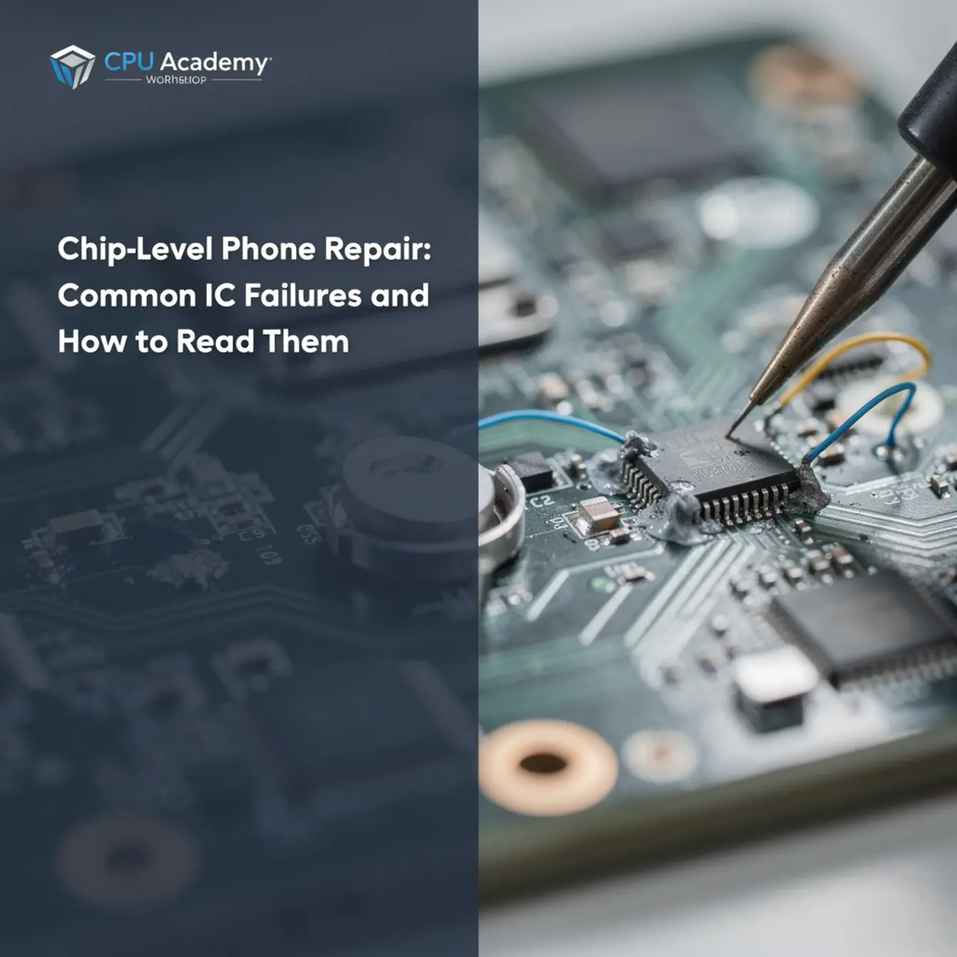
What Phone Chip-Level Repair Training Actually Covers
Phone chip-level repair training teaches technicians to diagnose and replace individual ICs — power management, baseband, audio, and charging chips — directly on the logic board. It requires reading schematics, using a microscope, and applying micro soldering skills. It opens higher-margin repairs that standard screen-swap technicians cannot offer.
That summary is the honest core of it. If you can already swap a screen or replace a charging port, chip-level work is the next layer down. You stop replacing whole boards and start fixing the exact component that failed.
This guide covers the minimum tools, the safety habits, and a repeatable five-step workflow. It also maps the most common IC failures to their symptoms so you know where to start probing instead of guessing.
What This Skill Is and When It Matters
Most phone repair shops operate at module level. Screen is cracked? Swap the screen. Charging port is bent? Replace the flex. That work is fast, teachable in days, and always in demand.
But a lot of phones come in where no module swap fixes the problem. The phone is dead. It charges to 1% and stops. The signal drops the moment the SIM is inserted. Those faults usually live on the logic board, in a chip the size of a grain of rice.
That is where chip-level repair earns its name. You work directly on the board — no module replacement, no whole-board swap. You find the failed IC, remove it cleanly, reball or replace it, and resolder it back in place.
The skill matters for two practical reasons. First, it lets you fix phones that your shop would otherwise return unfixed or write off. Second, board-level repairs carry higher ticket values because the knowledge barrier is real and most shops don’t offer it.
It is also honest work. You are not guessing. You are reading a schematic, following a voltage rail, and confirming the fault before you pick up a soldering iron.
Bench Setup, Tools, and Safety
You need the right tools before you touch a logic board. Working without them does not save time — it damages pads, lifts traces, and turns a one-chip job into a full board loss.
Your Core Tool List
| Tool | Why It Matters |
|---|---|
| Stereo or trinocular microscope | You cannot safely work on BGA pads without magnification. Period. |
| Hot-air rework station | Even heat distribution lets you lift a chip without scorching nearby components. |
| Fine-tip soldering iron | Used for pad repair, bridge removal, and through-hole work near ICs. |
| DC bench power supply with ammeter | Lets you spot a short by watching current draw before the battery is connected. |
| Multimeter | Continuity checks, diode mode testing, and resistance measurement on voltage rails. |
| Flux (rosin or no-clean) | Clean flux flow is what separates a smooth reflow from a bridged mess. |
| BGA reballing stencils | Required when a chip is lifted or its solder balls are damaged. |
| ESD mat and wrist strap | A single static discharge can kill a power management IC silently. |
| Phone jig or board holder | Boards that shift mid-rework cause pad damage and misaligned chips. |
| Isopropyl alcohol (90% or higher) | Flux residue under a BGA traps moisture and causes future faults. |
| Schematic and boardview software | Without a schematic you are guessing. With one, you are diagnosing. |
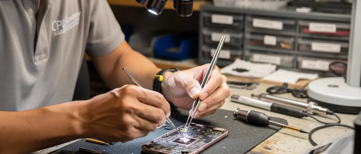
Microscope Setup
Mount the microscope so you can hold tools comfortably without bending your neck. Eye relief matters on long sessions. A trinocular head lets you attach a camera so you can document the board state before and after work — useful for customer records and for your own training review.
Heat Profile and Flux Choice
Every hot-air station is slightly different. Before you work on a customer board, run a test reflow on a donor board to learn your station’s true output at a given setting. Too much heat too fast lifts neighboring components. Too little heat leaves cold joints under the BGA.
For most smartphone ICs, a no-clean flux is the safer daily choice. It leaves less residue, and any residue that stays is non-conductive. Water-soluble flux flows better but demands a thorough cleaning pass — including under the chip — before the board is reassembled.
ESD and Pad Protection
Always wear your ESD strap when handling a bare logic board. Static discharge is invisible and the damage it causes often shows up as intermittent faults days after the repair. Keep your mat grounded and avoid synthetic clothing at the bench.
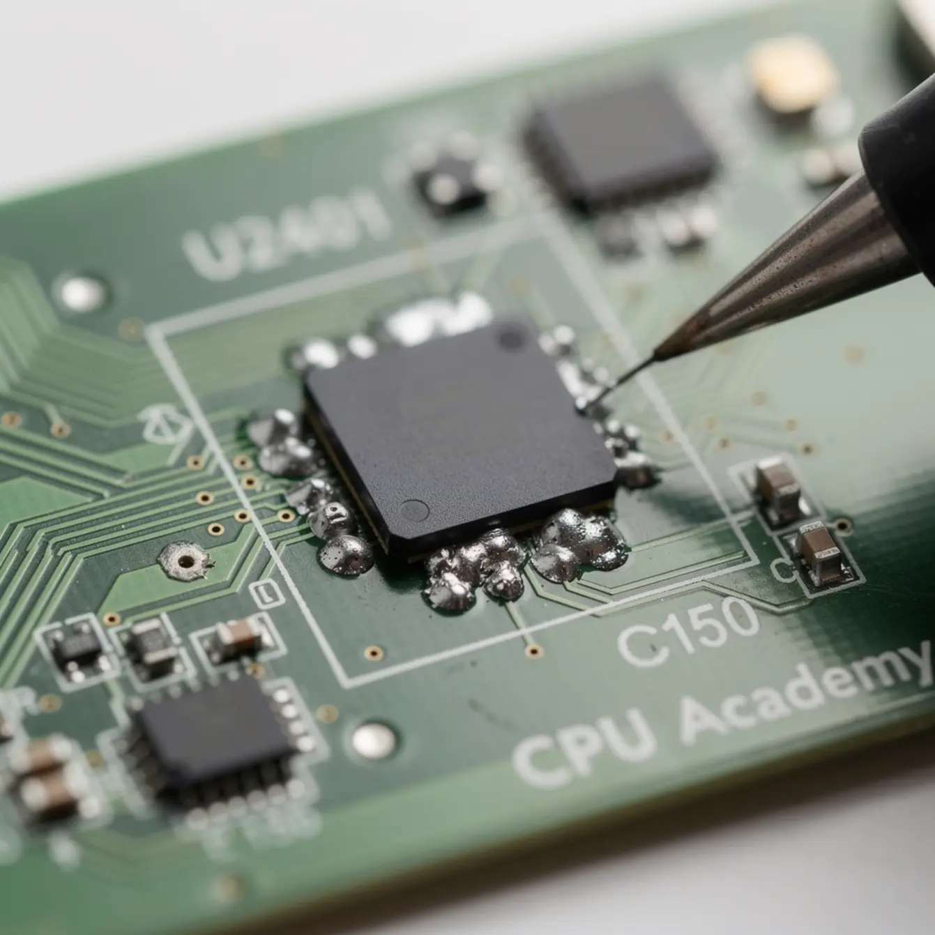
Before you remove any chip, inspect the pads under the microscope. Cracked, lifted, or corroded pads change the repair plan entirely. Trying to reball and replace a chip on damaged pads is how a one-hour job becomes a four-hour pad-rebuild session.
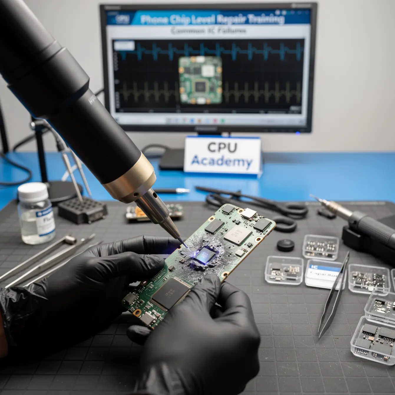
Core Workflow: 5 Steps from Symptom to Solder
A repeatable five-step workflow prevents random probing and protects the board from further damage. Follow it in order every time, even when the fault seems obvious.
- Record the symptom precisely. Note what the phone does and does not do: boots or no-boot, charges or no-charge, signal or no-signal. Write it down before touching the board. A clear symptom narrows the suspect IC immediately.
- Run a current draw test first. Connect the board to your DC bench supply at the phone’s nominal voltage and watch the ammeter. No current draw can mean an open fault. A high steady draw usually means a short. A current ramp that stops early often points to a power rail collapsing under load. This one reading tells you whether you are chasing a short, an open, or a logic fault.
- Pull the schematic before you probe anything. Find the rail associated with your suspect IC and trace it from the power source to the chip. This prevents you from probing blind and tells you exactly which test points are safe to touch. Schematic reading is not optional at this level — it is the method.
- Isolate the fault to one IC. Use diode mode on your multimeter to check rails feeding the suspect chip. Use freeze spray or a current-ramp thermal scan to locate hot spots. Confirm before removing. Removing the wrong chip damages good pads and wastes time.
- Remove, reball, replace, and verify. Apply flux, heat evenly, remove the chip cleanly, inspect and clean the pads, reball the replacement chip using the correct stencil, align under the microscope, reflow, and clean. Then power up through the bench supply again before reassembling. Verify the symptom is gone before the board goes back in the shell.
Common IC Failures, Mistakes, and Recovery
Most board-level faults cluster around a handful of ICs. Knowing the symptom-to-chip map cuts your diagnostic time significantly.
Fault Isolation by Symptom
| Symptom | Likely IC Suspect | First Diagnostic Step |
|---|---|---|
| Phone won’t power on, no boot | PMIC (Power Management IC), CPU power rail | Current draw test; check power rails on schematic |
| No charge, won’t sync to PC | Charging IC (tristar or hydra type, varies by model) | Measure voltage at charge port; diode mode on data lines |
| No cellular signal, IMEI missing | Baseband IC, RF transceiver | Software restore first; then check baseband power rails |
| Distorted audio, no microphone | Audio codec IC | Check audio codec supply rails; measure mic line resistance |
| Overheating, high idle current | Shorted component, PMIC stress | Freeze spray + slow current ramp to locate heat source |
| Touch unresponsive (display tests fine) | Touch IC | Check SPI communication lines on schematic |
| Camera fails to open or crashes | Camera module IC, ISP within AP | Isolate the module first; board-level only if module tests good |
| WiFi or Bluetooth absent | WLAN combo IC | Check crystal oscillator output and supply voltage |
Note: IC names, part numbers, and rail structures vary across manufacturers and model years. Always cross-reference the specific schematic for the device on your bench.
Rework QA: How to Confirm the Job Is Done Right
After reflowing a chip, do not reassemble immediately. Power up through the bench supply and repeat the current draw test. The draw should match normal boot behavior for that model. Then confirm the original symptom is resolved before the board goes back in the shell.
Check solder joints under the microscope at low magnification. Look for bridges, lifted edges, and uneven reflow patterns at the chip perimeter. BGA joints you cannot see directly — confirm them by function testing and, if available, X-ray inspection on high-value boards.
- Removing a chip before confirming it is the fault. Current draw testing and schematic rail checks come first, always.
- Using too much flux. Excess flux runs under nearby components and creates leakage paths. A small, precise amount is enough.
- Skipping the pad inspection step. Damaged pads must be repaired before a new chip is placed. Placing a chip on a cracked pad just delays failure.
- Overheating the board. Sustained high heat lifts pads, delaminates the board, and destroys adjacent passives. Learn your station’s true temperature at the board surface, not just the dial setting.
- Skipping ESD precautions because the repair “looks simple.” ESD damage is cumulative and silent. It shows up later as intermittent faults that are almost impossible to trace.
How Schematic Thinking Speeds Diagnosis
Every fault you will encounter on a logic board has a path. Voltage enters the board, travels through rails, passes through regulators, and arrives at each IC in the correct amount. When something fails, that path breaks or shorts somewhere along the route.
A schematic is the complete map of those paths. Without it, you are touching test points and hoping. With it, you know which node to probe, what voltage to expect, and which direction the fault is most likely sitting.
The Practical Connection Between Schematics and Micro Soldering
Micro soldering training and schematic reading are not separate skills. They are the same skill viewed from two angles. The schematic tells you which chip to target. The soldering skill lets you act on that information without creating new damage.
A technician who can solder but cannot read a schematic is guessing at components. A technician who can read schematics but cannot solder cleanly cannot execute the fix. You need both to work confidently at board level.
A good micro soldering course builds both together, using real board faults and real schematics so the connection between theory and bench work is always visible. That is what separates structured micro soldering classes from watching random repair videos and hoping the pattern repeats.
If you want to see how schematic reading maps directly to board-level iPhone and Android faults, CPU Academy’s Phone Schematic Diagram Course: Master iPhone & Board Repair is built specifically for that transition — giving working technicians the structured reading framework they need before they start probing live boards.
A Real Repair Case: No-Charge Fault
Board received: iPhone, no-charge fault. Customer reports phone stopped charging after a drop.
Current draw test: 0mA at 5V input. No draw at all.
Schematic check: Voltage rail feeding charging IC showed correct input but no output on the secondary rail. Charging IC confirmed as suspect.
Pad inspection: One pad showing micro-crack consistent with impact damage. Pad rebuilt with silver conductive epoxy before chip placement.
Resolution: Charging IC replaced under microscope. Reflow verified. Normal charge current confirmed on bench supply before reassembly. Phone returned to customer charging normally.
This is a repeatable process, not a lucky guess. The schematic told the technician where to look. The bench supply confirmed the fix. The microscope made the execution safe.
Board-Level Repair as a Career Move
A board level phone repair course, or a full BGA rework phone repair course, adds a tier of service that the majority of independent shops cannot match. You become the shop that takes the jobs others send away. That is a real business advantage, and it compounds over time as your diagnostic speed improves.
If you are working toward that goal, the supporting knowledge base matters. Understanding software faults before blaming hardware saves unnecessary board work — CPU Academy’s mobile phone software repair course covers that layer. And if you are building a repair business around these skills, the starting a mobile phone repair business course covers the operational side.
FAQ
Do I need prior electronics experience to start phone chip-level repair training?
Basic familiarity with phone repair helps, but formal electronics training is not required. What matters is understanding how to use a multimeter, following instructions carefully, and practicing patience under magnification. Most people enter this skill level after doing module-level repairs for at least a few months.
What is the hardest part of chip-level work for beginners?
Reading schematics is the steepest early curve. Micro soldering itself becomes mechanical with practice, but understanding what the schematic is showing you — which rail feeds which chip, what normal voltage looks like — takes deliberate study. That is why pairing a micro soldering course with formal schematic training makes the learning curve much shorter.
What does BGA reballing actually involve?
BGA stands for Ball Grid Array. The solder connections on a BGA chip are tiny balls of solder on the underside of the chip. When a chip is removed, those balls are usually destroyed. Reballing means cleaning the chip pads, placing a stencil sized to that chip, applying new solder paste, and reflowing to create fresh balls. The chip is then realigned on the board and reflowed into place.
How is chip-level repair different from a standard phone repair course?
A standard phone repair course teaches module-level work: screen replacements, battery swaps, port replacements. Chip-level repair goes deeper — you are working on the logic board itself, targeting individual ICs. The tools, the diagnostic method, and the knowledge required are all more advanced. The two skill sets complement each other rather than replace one another.
Is chip-level repair worth learning if I already run a repair shop?
Yes, if your shop currently returns dead boards unfixed or pays wholesale to send them out. Board-level work converts those lost jobs into shop revenue. The tools have an upfront cost, and the learning curve is real, but technicians who add this skill consistently report higher-ticket repairs and a category of customers who have no other local option.
Do I need to learn schematic reading before I start micro soldering?
They can be learned in parallel, but schematic reading should come first for diagnostic work. You can practice soldering technique on donor boards without schematics, but you cannot safely diagnose a live fault without knowing where to probe. Start schematic reading as early as possible in your training.